Systems and methods for nanomaterial transfer

a technology of nanomaterials and nanomaterials, applied in the field of nanomaterials, can solve the problems of increasing complexity of these devices, difficult or impossible to directly process on or with materials, and equally challenging discoveries, etc., and achieve the effect of high compatibility and efficient operation

Active Publication Date: 2008-11-20
GEORGIA TECH RES CORP
View PDF5 Cites 62 Cited by
  • Summary
  • Abstract
  • Description
  • Claims
  • Application Information

AI Technical Summary

Problems solved by technology

Electronic devices are responsible for the majority of advancements in technology in the last century, and the complexity of these devices grows in proportion to the exponential advancements in the field.
Recent discoveries with respect to nanomaterials have opened new doors with respect to enabling durable, robust, and flexible electronic devices, but these new discoveries come with equally challenging obstacles.
One of the significant challenges encountered with use of nanomaterials in electronic devices relates to a dichotomy between conductive and flexible materials.
Typically materials that have excellent transport properties, regarding conductivity and carrier mobility, are difficult or impossible to directly process on or with materials that are flexible, malleable, and durable.
In accordance with this dichotomy, nanomaterial structures that have excellent transport or structural properties, such as carbon nanotubes or semiconductor nanowires, are difficult to process and fabricate with flexible, malleable, and durable materials such as polymer substrates.
As nanomaterial structures, such as carbon nanotubes and semiconductor nanowires, are the product of recent discoveries, their applications and uses are widely undeveloped and undiscovered.
Laser ablation typically produces a small amount of clean nanotubes, whereas arc discharge methods generally produce large quantities of impure material.
Despite its advantages, the use of amorphous silicon in flexible electronic devices has significant drawbacks.
For instance, in general, the processing temperature requirements for amorphous silicon limit its compatibility to a small number of polymers.
Furthermore, the low transport mobility of amorphous silicon, on the order of 1 cm2 / Vs, limits the applications in which the resulting flexible electronic device can be utilized.
Unfortunately, many problems exist in the compatibility of CNTs with flexible polymer substrates.
More specifically, the synthesis of CNTs directly onto polymer substrates is not feasible due to the high temperatures or harsh chemical environments under which they are synthesized.
Many problems exist with the solution-based CNT transfer methods, such as the methods disclosed in Chang, et al., Yaniv, et al. and Blanchet-Fincher, due to, among other things, the fact that the carbon nanotubes are fragile, vulnerable to separation, and randomly oriented in the solution.
This random orientation of the CNTs can be detrimental to many applications, including creating non-optimized electrical field distribution and resulting in shielding effects between adjacently positioned CNTs.
This significantly limits the choice of ink and solvents and the choice of polymers.
Furthermore, the flexible electronic devices created by these solution-based transfer methods are very vulnerable, due to the fact that the CNTs simply reside on the surface of the substrate to which they applied.
The development of solution-based CNT transfer inks require extensive fabrication time cycles.
The create of the ink requires a significant amount of time to disperse the CNTs throughout the solution.
Even after the solution has been applied to the substrate, the solution must be printed and the “solvent” evaporated (requiring more processing time).
Similar problems are encountered in the manufacture of flexible electronic devices that incorporate nanomaterial structures other than CNTs.
For example, known methods for the incorporation of nanowires into flexible polymer substrates suffer from the same problems as the described conventional methods for CNT transfer.
In transferring the nanowires to a polymer substrate, the integrity of the nanowire structure is often lost or degraded and the nanowires are only tenably attached to the polymer substrate.

Method used


Image

  • Systems and methods for nanomaterial transfer
  • Systems and methods for nanomaterial transfer
  • Systems and methods for nanomaterial transfer

Examples


Embodiment Construction

[0054]To facilitate an understanding of the principles and features of the invention, it is explained hereinafter with reference to its implementation in illustrative embodiments. In particular, the present invention is directed toward systems and methods for nanomaterial transfer.

[0055]Referring now to the figures, wherein like reference numerals represent like parts throughout the several views, exemplary embodiments of the present invention will be described in detail. Throughout this description, various components may be identified having specific values, these values are provided as exemplary embodiments and should not be limiting of various concepts of the present invention as many comparable sizes and / or values may be implemented.

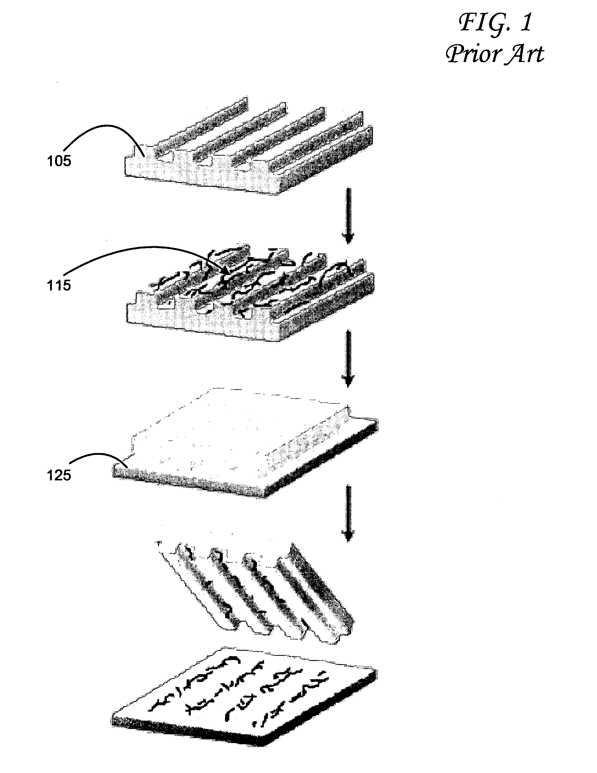
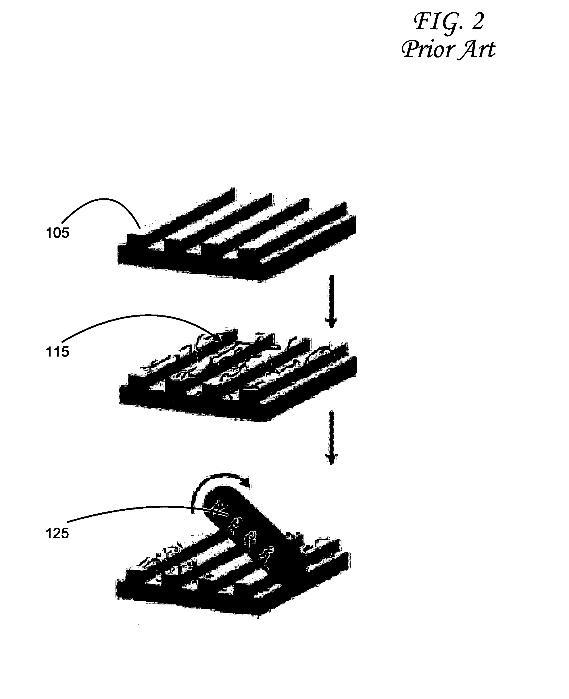
[0056]FIG. 1 is an illustration of a prior art method of transferring carbon nanotubes to a polymer substrate. The conventional solution-based method illustrated in FIG. 1 utilizes a Polydimethylsiloxane (PDMS) applicator 105. PDMS is a widely used ...


PUM

PropertyMeasurementUnit
diameteraaaaaaaaaa
tensile strengthaaaaaaaaaa

Abstract

Systems and methods of nanomaterial transfer are described. A method of nanomaterial transfer involving fabricating a template and synthesizing nanomaterials on the template. Subsequently, the nanomaterials are transferred to a substrate by pressing the template onto the substrate. In some embodiments, the step of transferring the nanomaterials involves pressing the template onto the substrate such that the nanomaterials are embedded below a surface layer of the substrate. In some embodiments, the temperature of the plurality of nanomaterials is raised to assist the transfer of the nanomaterials to the substrate.

Description

CROSS REFERENCE TO RELATED APPLICATIONS[0001]This application claims priority of U.S. Provisional Patent Application No. 60 / 691,566, filed Jun. 17, 2005, the entire contents and substance of which are hereby incorporated by reference.BACKGROUND[0002]1. Field of the Invention[0003]The present invention relates to a nanomaterials and, more particularly, to flexible devices containing nanomaterials.[0004]2. Description of Related Art[0005]Electronic devices are responsible for the majority of advancements in technology in the last century, and the complexity of these devices grows in proportion to the exponential advancements in the field. As electronic devices continue to expand into every facet of everyday life, the demand for more durable, robust, and flexible electronic devices becomes increasingly significant. Recent discoveries with respect to nanomaterials have opened new doors with respect to enabling durable, robust, and flexible electronic devices, but these new discoveries c...

Claims


Application Information

Patent Timeline
Patent Type & Authority Applications(United States)
IPC IPC(8): H05K1/09B29C65/70
CPCB81C1/00031B81C2201/0185B82Y10/00B82Y30/00B82Y40/00G03F7/0002Y10S977/707Y10S977/887
Inventor GRAHAM, JR., SAMUELKING, WILLIAM P.WONG, CHING-PING
Owner GEORGIA TECH RES CORP
Why Eureka
Try Eureka