
Semiconductor Device and Its Fabrication Method

a technology of semiconductor devices and fabrication methods, applied in semiconductor devices, semiconductor/solid-state device details, electrical apparatus, etc., can solve the problems of increasing the fabrication cost, affecting the quality of electrical connection between the chips and the substrate, and reducing the efficiency of the chip integration. , to achieve the effect of enhancing the electrical function, and reducing the number of dies

Inactive Publication Date: 2008-11-20
SILICONWARE PRECISION IND CO LTD
View PDF4 Cites 36 Cited by
  • Summary
  • Abstract
  • Description
  • Claims
  • Application Information

AI Technical Summary

Benefits of technology

[0011]In view of the disadvantages of the prior art mentioned above, it is an objective of the present invention to provide a semiconductor device and a fabrication method thereof, through which more chips can be integrated in a semiconductor package without increasing die attachment area.
[0012]It is another objective of the present invention to provide a semiconductor device and a fabrication method thereof that provide a simple fabrication process, thereby avoiding complicated fabrication process and high production cost caused by using the TSV technique.
[0013]It is a further objective of the present invention to provide a semiconductor device and a fabrication method thereof through which a plurality of chips can be directly electrically connected to one another, thereby avoiding poor electrical performance caused by using the wire bonding technique.
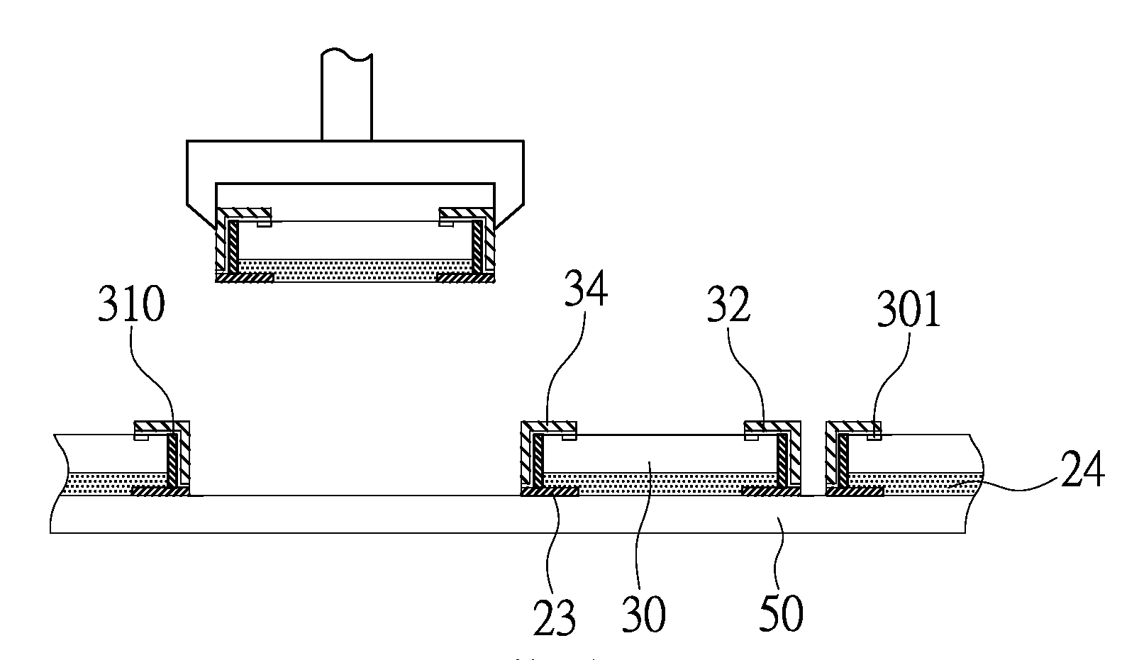
[0019]In the subsequent fabrication process, the conductive circuits of a semiconductor device can be thermally compressed and electrically connected to a substrate or the metal layer of another semiconductor device so as to form a 3-D multi-chip stack structure. Thus, the present invention is capable of efficiently integrating more chips to enhance electrical function without increasing die attachment area. Moreover, the present invention not only avoids poor electrical performance caused by using the wire bonding technique but also avoids complicated fabrication process and high fabrication cost caused by using the TSV technique.

Problems solved by technology

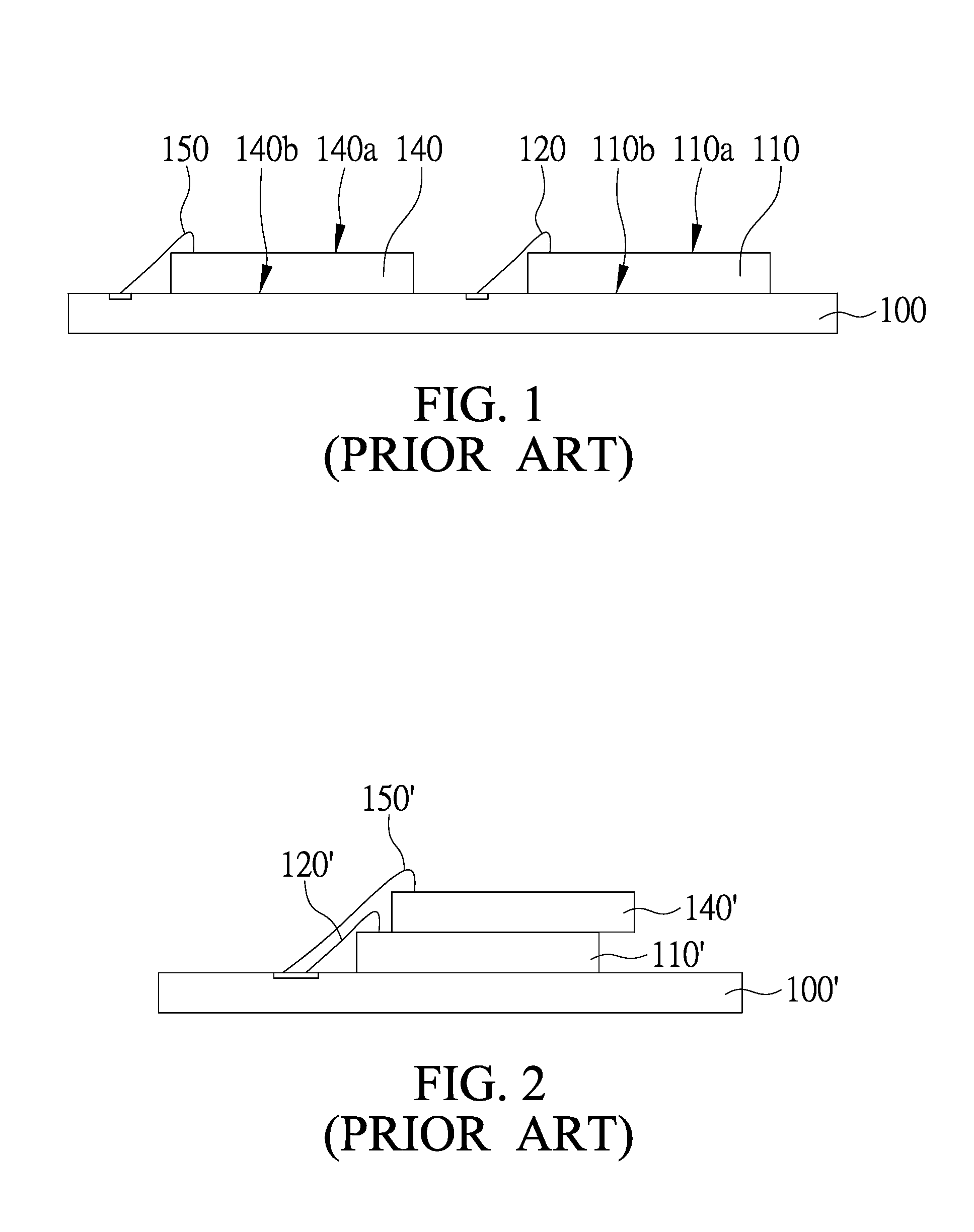
A major disadvantage of the aforementioned multi-chip semiconductor package is that the chips must be spaced apart from each other at a certain distance so as to prevent miscontact between the conductive wires of the adjacent chips.
Thus, when a plurality of chips are mounted to a substrate, a large die attachment area is required on the substrate to accommodate the chips, thereby increasing the fabrication cost and making it difficult to obtain thinner, lighter and smaller packages.
Although such a stack structure can save more substrate space than the abovementioned semiconductor package with horizontally spaced chips, it still requires a wire bonding technique to electrically connect the chips to the substrate.
As a result, quality of electrical connection between the chips and the substrate would be adversely affected by length of bonding wires.
However, as the TSV technique has a complicated fabrication process and high fabrication cost, its application value in the industry is quite limited.

Method used


Image

  • Semiconductor Device and Its Fabrication Method
  • Semiconductor Device and Its Fabrication Method
  • Semiconductor Device and Its Fabrication Method

Examples


first embodiment

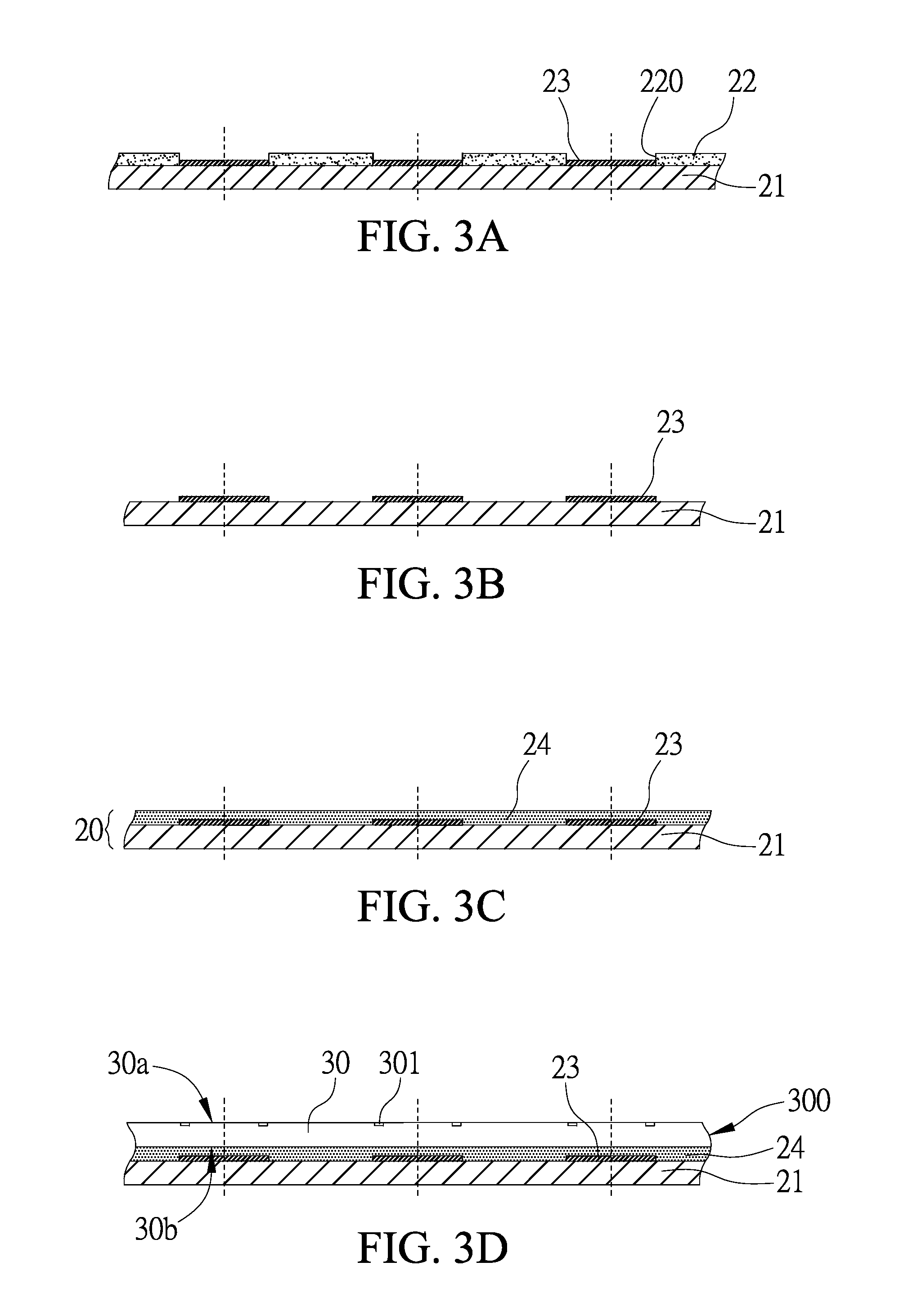
[0029]Please refer to FIGS. 3A through 3L, which are diagrams of a semiconductor device and a fabrication method thereof according to the first embodiment of the present invention.

[0030]As shown in FIGS. 3A through 3C, a bottom board 21 made of such as copper (Cu) is provided. A first resist layer 22 is formed on the bottom board 21, a plurality of apertures 220 are formed in the first resist layer 22 to expose part of the bottom board 21, and a plurality of conductive circuits 23 made of such as gold / palladium / nickel (Au / Pd / Ni) are formed in the apertures 220 by electroplating. The first resist layer 22 is removed, and an insulating layer 24 is formed on the bottom board 21 to cover the conductive circuits 23 and the bottom board 21. The insulating layer 24 is made of such as B-stage epoxy resin or polyimide. Thus, a carrier board 20 that includes the bottom board 21, the plurality of conductive circuits 23 on the bottom board 21, and the insulating layer 24 that covers the bottom ...

second embodiment

[0045]Please further refer to FIGS. 5A through 5D, which are diagrams of a semiconductor device and a fabrication method thereof according to the second embodiment of the present invention. For simplification, elements of the present embodiment that are same as or similar to those of the first embodiment are denoted with the same reference numerals.

[0046]As shown in FIGS. 5A and 5B, the semiconductor device and its fabrication method of the present embodiment are mostly similar to the first embodiment, the main difference therebetween is that after the metal layer 34 made of, for example copper / solder (Cu / Solder) or nickel / solder (Ni / Solder) is formed, a dielectric layer 35 is further formed on the active surfaces of the chips and the metal layer. The dielectric layer 35 is made of polyamide or an epoxy resin, for example.

[0047]As shown in FIG. 5C, the bottom board 21 is removed by means of etching, and a solder mask layer 36 such as green paint is formed on the insulating layer 24,...


PUM


Abstract

A semiconductor device and a fabrication method thereof are disclosed. The method includes attaching a wafer with a plurality of chips on a carrier board having an insulating layer, a plurality of conductive circuits and a bottom board; forming a plurality of first grooves between solder pads of adjacent chips to expose the conductive circuits, and filling the first grooves with an insulating adhesive layer; forming second grooves in the insulating adhesive layer; and cutting among the chips to separate the chips from one another.

Description

BACKGROUND OF THE INVENTION[0001]1. Field of the Invention[0002]This invention generally relates to semiconductor devices and fabrication method thereof, and more specifically, to semiconductor devices capable of being vertically stacked and fabrication method thereof.[0003]2. Description of Related Art[0004]Conventional semiconductor packages are generally presented as a form of multi-chip module (MCM), wherein at least two chips are mounted on a substrate or a lead frame of a single semiconductor package.[0005]Please refer to FIG. 1, which illustrates a conventional multi-chip semiconductor package with horizontally spaced chips. As shown in FIG. 1, the semiconductor package includes a substrate 100, a first chip 110 having an active surface 110a and an opposite non-active surface 110b, wherein the non-active surface 110b of the first chip 110 is adhered to the substrate 100 and the active surface 110a of the first chip 110 is electrically connected to the substrate 100 via first ...

Claims


Application Information

Patent Timeline
Patent Type & Authority Applications(United States)
IPC IPC(8): H01L23/488H01L21/304
CPCH01L21/568H01L21/6835H01L2924/07802H01L24/27H01L2225/1058H01L2225/1035H01L2924/01033H01L23/3128H01L24/97H01L25/0657H01L25/105H01L25/50H01L2221/68345H01L2224/274H01L2224/48091H01L2224/97H01L2225/06513H01L2225/06551H01L2225/06562H01L2924/01013H01L2924/01029H01L2924/01046H01L2924/01074H01L2924/01079H01L2924/01082H01L2924/15184H01L2924/15311H01L2924/15331H01L24/48H01L2924/01005H01L2924/01006H01L2924/01023H01L2924/00014H01L2924/00H01L2224/45099H01L2224/45015H01L2924/207
Inventor HUANG, CHIEN-PINGCHANG, CHIN-HUANGHUANG, CHIH-MING
Owner SILICONWARE PRECISION IND CO LTD
Learn More