Semiconductor device and method for manufacturing the same
- Summary
- Abstract
- Description
- Claims
- Application Information
AI Technical Summary
Benefits of technology
Problems solved by technology
Method used
Image


Examples
Embodiment Construction
[0021]A semiconductor device according to the embodiments of the present invention and a method for manufacturing the same will be described with reference to the drawings.
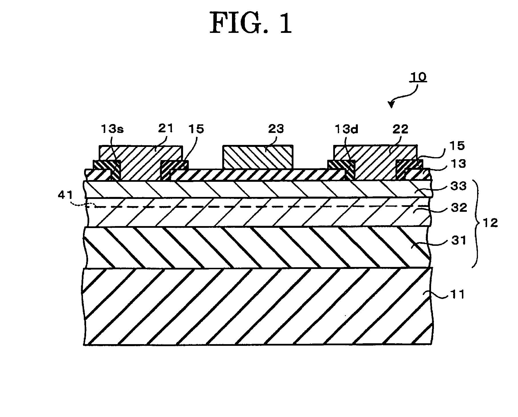
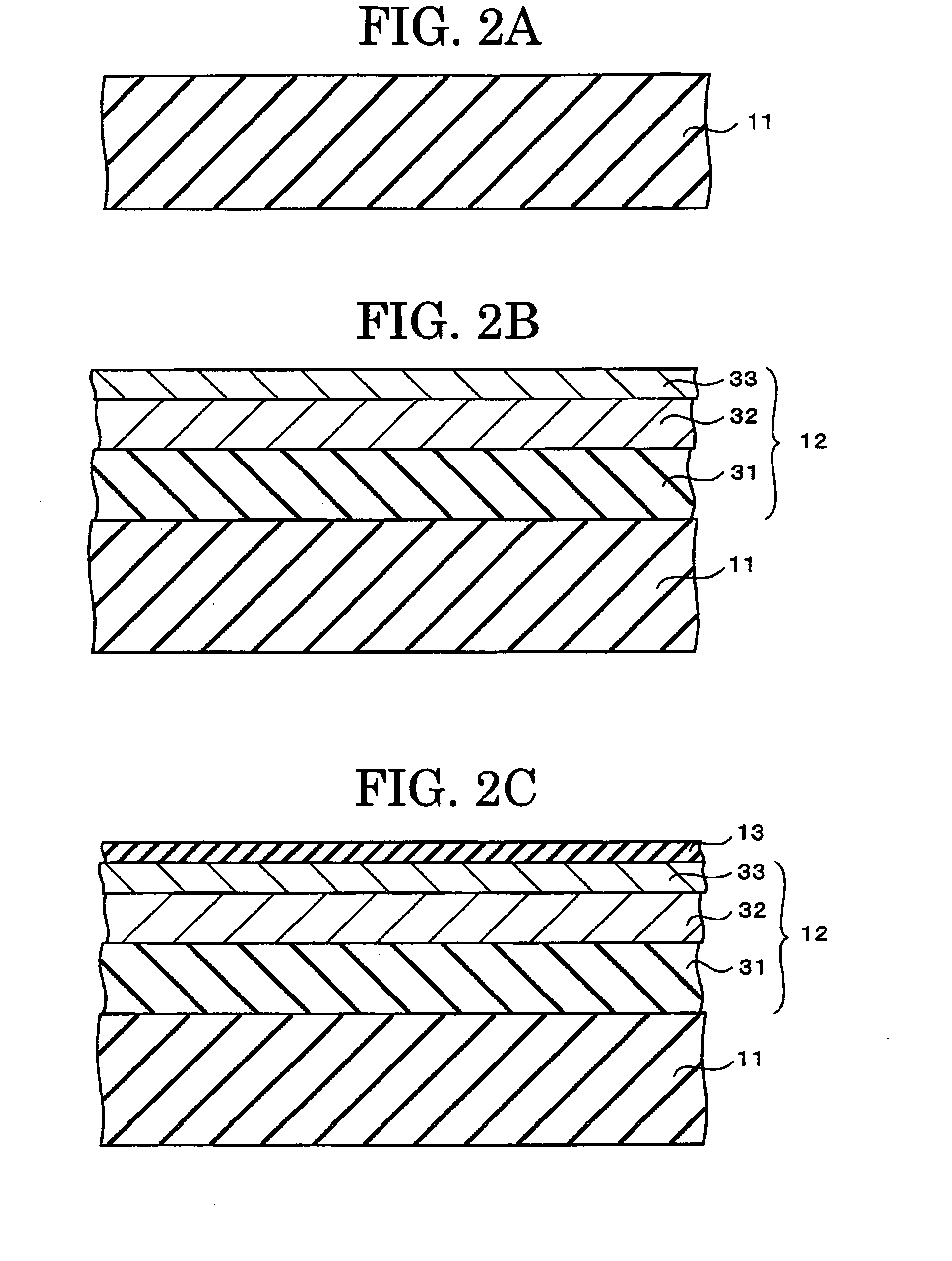
[0022]A semiconductor device 10 according to an embodiment of the present invention and a method for manufacturing the same are shown in FIGS. 1, 2A, 2B, 2C, 2D, and 2E. Here the description will be given with a High Electron Mobility Transistor (HEMT) taken as an example of the semiconductor device according to the embodiment. FIG. 1 is cross-sectional view showing an exemplary structure of the semiconductor device 10 according to the embodiment.
[0023]The semiconductor device 10, as shown in FIG. 1, comprises a substrate 11, a semiconductor layer 12, an insulation film 13, a protective film 15, a source electrode 21, a drain electrode 22 and a gate electrode 23.
[0024]The substrate 11 is formed of, for example, Si monocrystal. The substrate 11 serves as a substrate for growing the semiconductor layer 12 by epitaxy...
PUM
 Abstract
Description
Claims
Application Information
 - Generate Ideas
- Intellectual Property
- Life Sciences
- Materials
- Tech Scout
- Unparalleled Data Quality
- Higher Quality Content
- 60% Fewer Hallucinations
Browse by: Latest US Patents, China's latest patents, Technical Efficacy Thesaurus, Application Domain, Technology Topic, Popular Technical Reports.
© 2025 PatSnap. All rights reserved.Legal|Privacy policy|Modern Slavery Act Transparency Statement|Sitemap|About US| Contact US: help@patsnap.com