Simultaneous design of integrated circuit and printed circuit board

a technology of integrated circuits and printed circuit boards, which is applied in the direction of printed circuits, program control, instruments, etc., can solve the problems of cumbersome design of pcb circuit assemblies, less than optimal, and cost addition, and achieve optimal pcb circuit assembly design

Inactive Publication Date: 2008-11-20
MIRROR SEMICON
View PDF9 Cites 47 Cited by
  • Summary
  • Abstract
  • Description
  • Claims
  • Application Information

AI Technical Summary

Benefits of technology

[0011]In view of the circumstances noted above, an aspect of at least one of the embodiments disclosed herein is to provide a PCB circuit a...

Problems solved by technology

While application specific integrated circuits (ASICs) can be used, they are expensive and thus the current state of the art for designing most PCB circuit assemblies is constrained by the designer having to use only “standard” off-the-shelf components along with CAD (EDA) software, which may be modified by the designer's knowledge and experience to give special attention to the best possible path when connecting the pins of one component to those of another.
Though simple PCB circuit assembly designs that comprise a small number of components and a limited number of connections between pins can be ac...

Method used


Image

  • Simultaneous design of integrated circuit and printed circuit board
  • Simultaneous design of integrated circuit and printed circuit board
  • Simultaneous design of integrated circuit and printed circuit board

Examples


Embodiment Construction

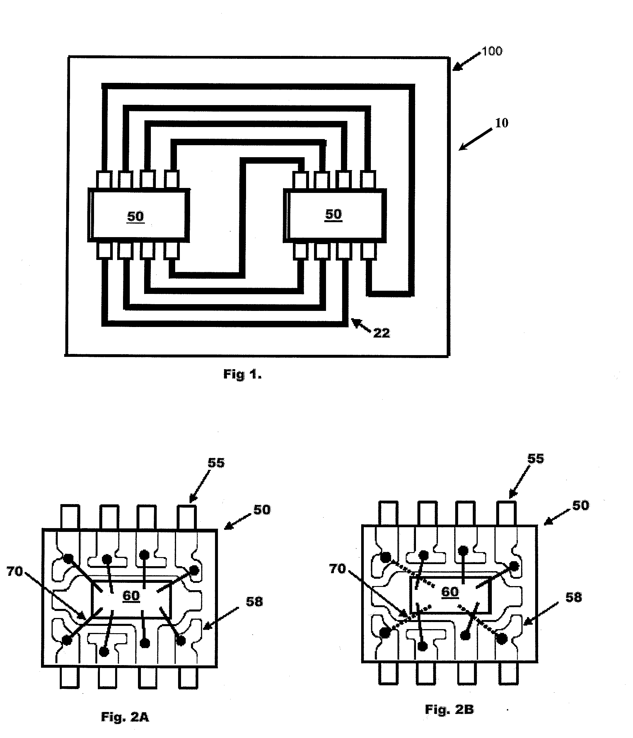
[0027]FIG. 1 schematically illustrates a printed circuit board (PCB) circuit assembly 100. The PCB circuit assembly 100 includes a PCB 10 with a variety of components mounted thereon, including at least one integrated circuit (IC) package 50. Traces 22, which can be made of copper or another suitable metallic conductor, define the circuit routing layout on the PCB 10 between the different components. Though only two IC packages 50 are shown in FIG. 1, one of ordinary skill in the art will recognize that the PCB circuit assembly can include a variety of components (e.g., resistors, capacitors, diodes), in addition to the IC packages 50, and that the number of components can vary as needed for the particular PCB circuit assembly.

[0028]FIGS. 2A-B are schematic illustrations of one embodiment of an IC package 50. In the illustrated embodiment, the IC package 50 includes an IC die 60 (e.g., silicon chip) coupled to an interposer substrate (or lead frame) 58 via a plurality of bond wires ...


PUM


Abstract

A printed circuit board (PCB) circuit assembly is designed utilizing software to create the best performing “total design” by selecting component layout locations, optimizing the circuit routing of the PCB copper (or other metallic) traces, and simultaneously optimizing the interconnections between a “standard” die inside an integrated circuit (IC) package and an interposer substrate of the IC package.

Description

CROSS-REFERENCE TO RELATED APPLICATIONS[0001]The present application is based on and claims priority to U.S. Provisional Application No. 60 / 938,097, filed May 15, 2007, the entire contents of which are incorporated by reference and should be considered a part of this specification.BACKGROUND OF THE INVENTION[0002]1. Field of the Invention[0003]The present invention relates to printed circuit boards (PCB) and integrated circuit (IC) packaging technology for semiconductor devices, and more particularly to the field of electronic interconnection structures of ICs, and / or IC packages, and PCBs and the simultaneous design of the same.[0004]2. Description of the Related Art[0005]In the fields of electronic and electrical devices, most manufactured products comprise a variety of sub-components that require interconnection. At the present, it is estimated that more than 90% of PCB board level designs use standard “commercial off-the-shelf” (COTS) components. These components include discret...

Claims


Application Information

Patent Timeline
IPC IPC(8): G06F17/50
CPCG06F17/5077H05K1/181H05K3/0005H05K2201/09227H05K2201/10689H05K2201/10734G06F30/394H01L2224/48247H01L2224/48471H01L2224/4917H01L2224/49171
Inventor HART, MARTINFJELSTAD, JOSEPH C.
Owner MIRROR SEMICON
Why Eureka
Try Eureka