Flat Panel Display

a technology of display panel and flat panel, applied in the field of flat panel display, can solve the problems of high cost of laser device, substrate deformation easily by heat treatment at a high temperature, and long process time, and achieve the effect of preventing the image quality of the display panel

Active Publication Date: 2008-11-27
SEOUL NAT UNIV R&DB FOUND
View PDF4 Cites 13 Cited by
  • Summary
  • Abstract
  • Description
  • Claims
  • Application Information

AI Technical Summary

Benefits of technology

[0006]Accordingly, an object of the present invention is to provide a flat panel display that can prevent image quality of a display panel from being degraded by a leakage current of each pixel circuit.

Problems solved by technology

The solid phase crystallization method has problems that its process time is too long and a substrate is easily deformed by heat treatment at a high temperature for a long time.
The excimer laser crystallization method capable of low temperature crystallization has disadvantages in that it requires an expensive laser device and an interfacial property between a semiconductor layer and a gate insulation film is bad due to extrusions formed on the poly-crystallized surface.
When the metal induced crystallization or metal induced lateral crystallization is used, metal catalysts remain in a crystallized silicon layer, thereby increasing leakage current of the semiconductor layer of the thin film transistor.
However, most of newly proposed methods have a problem that the leakage current of the thin film transistor is very high.
Thus, it is very difficult to use the methods actually in products.
In addition, even if the same data voltage is applied to the drain of the thin film transistor, image quality degradation phenomenon such as change of brightness and degradation of image quality is caused by difference between leakage currents of each pixel.

Method used


Image

  • Flat Panel Display
  • Flat Panel Display
  • Flat Panel Display

Examples


Embodiment Construction

[0037]Hereinafter, preferred embodiments of the present invention will be described in detail with reference to the accompanying drawing. The aspects and features of the present invention and methods for achieving the aspects and features will be apparent by referring to the embodiments to be described in detail with reference to the accompanying drawings. However, the present invention is not limited to the embodiments disclosed hereinafter, but can be implemented in diverse forms. The matters defined in the description, such as the detailed construction and elements, are nothing but specific details provided to assist those of ordinary skill in the art in a comprehensive understanding of the invention, and the present invention is only defined within the scope of the appended claims. In the entire description of the present invention, the same drawing reference numerals are used for the same elements across various figures.

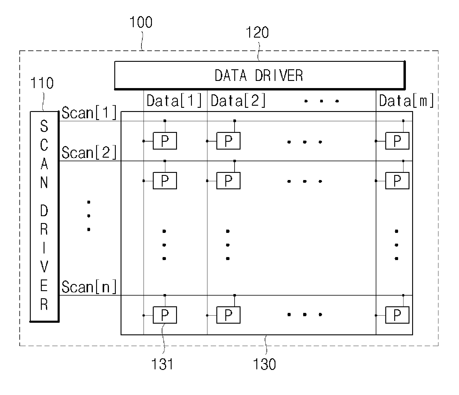
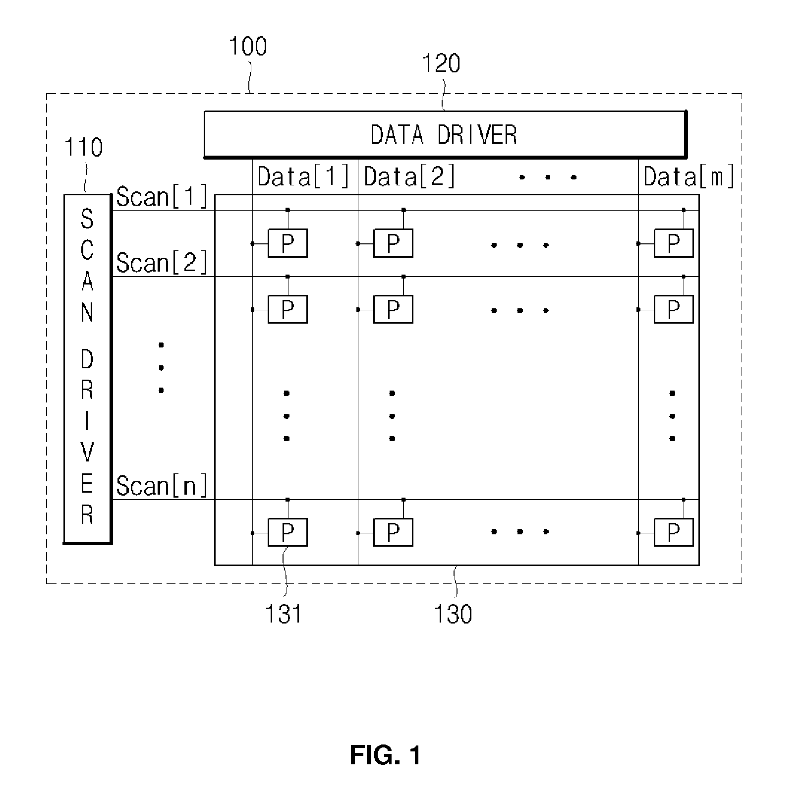
[0038]FIG. 1 shows a block diagram illustrating a construc...


PUM

PropertyMeasurementUnit
voltageaaaaaaaaaa
voltagesaaaaaaaaaa
capacitanceaaaaaaaaaa

Abstract

Disclosed is a flat panel display that can prevent image quality degradation by preventing the current transmitted to the organic light emitting diode or liquid crystal of the flat panel display from being changed by the leakage current and keeping the current stably. The flat panel display comprises: a first switching element whose control electrode is electrically coupled to a scan line, being electrically coupled between a data line and a first voltage line; a second switching element whose control electrode is electrically coupled to the scan line, being electrically coupled between the first switching element and first voltage line; a capacitive element whose first electrode is electrically coupled between the first and second switching elements; a drive transistor whose control electrode is electrically coupled to the second switching element, being electrically coupled between the first voltage line and a second voltage line; and an organic light emitting diode electrically coupled between the drive transistor and second voltage line.

Description

FIELD OF THE INVENTION[0001]The present invention relates to a flat panel display, and more particularly, to a flat panel display that can minimize degradation of image quality caused by leakage current of a pixel circuit.BACKGROUND OF THE INVENTION[0002]A flat panel display includes a passive matrix (PM) type and an active matrix (AM) type using a MOS (Metal Oxide Silicon) thin film transistor (TFT). In the active matrix (AM) type flat panel display, a thin film transistor and a capacitive element are connected to respective ITO (indium tin oxide) pixel electrodes for keeping voltages by capacitance of capacitors. The active matrix type flat panel display is widely used according to tendency of high resolution.[0003]The thin film transistor used in the active matrix type flat panel display is generally classified into a poly-silicon thin film transistor and an amorphous silicon thin film transistor according to a kind of an active layer. The poly-silicon thin film transistor has hi...

Claims


Application Information

Patent Timeline
Patent Type & Authority Applications(United States)
IPC IPC(8): G02F1/133G09G3/32
CPCG02F1/13624G09G3/3225G09G3/3648G09G2300/0814G09G2320/0233G09G3/20G09G3/30G09G3/36
Inventor HAN, MIN KOOPARK, HUYN SANG
Owner SEOUL NAT UNIV R&DB FOUND
Why Eureka
Try Eureka