Electro-optic substrate, electro-optic device, method of designing the electro-optic substrate, and electronic device
a technology of electrooptic substrates and electrooptic devices, applied in the direction of semiconductor devices, instruments, electrical devices, etc., can solve problems such as deterioration in the displayed image quality, and achieve the effect of excellent visibility and high intensity
- Summary
- Abstract
- Description
- Claims
- Application Information
AI Technical Summary
Benefits of technology
Problems solved by technology
Method used
Image

Examples
first embodiment
[0046]Hereinafter, a first embodiment will be described with reference to the drawings.
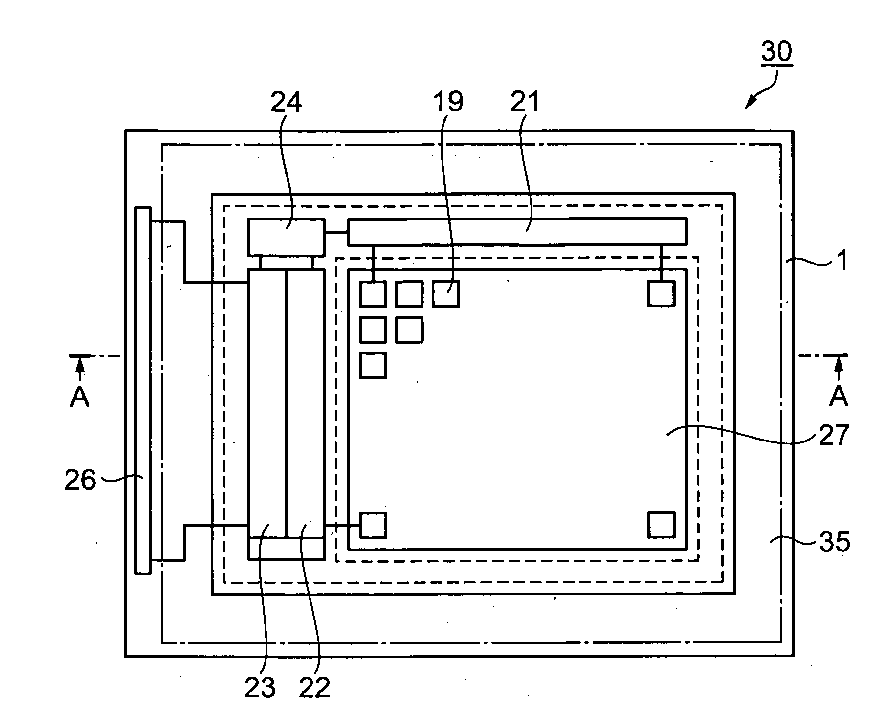
[0047]FIG. 1 is a plane view of an electro-optic substrate including a thin-film transistor. A thin-film transistor 205 is driven with electric power transmitted through a signal wire 9 and a gate wiring 6. A drain electrode 8 is coupled to a pixel electrode 19 using ITO to control the potential of the pixel electrode 19.
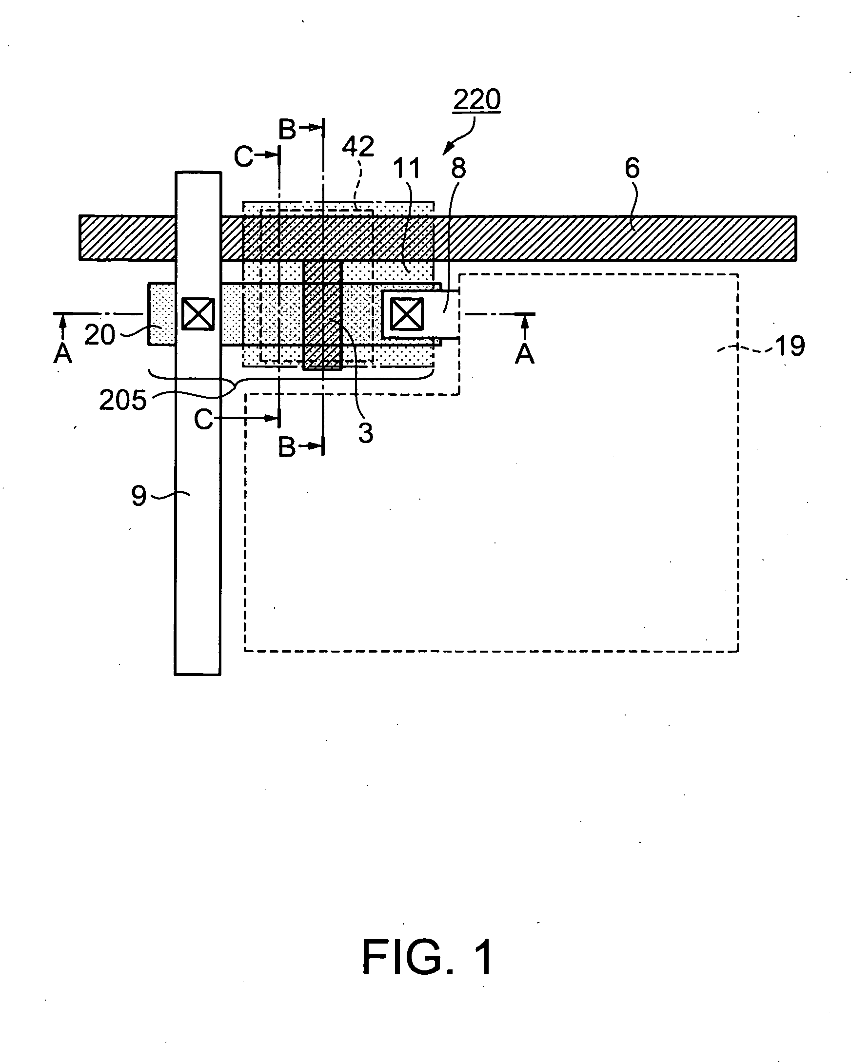
[0048]FIG. 2 is a cross-sectional view of FIG. 1 along the line A-A. Herein, a configuration which is not affected by stray light is omitted. A quartz substrate 1 as a transparent substrate is provided with a second light-shielding layer 4 using tungsten silicide. The second light-shielding layer 4 may have a thickness of about 100 to 1000 nm, for example. Herein, instead of the tungsten silicide, the second light-shielding layer 4 may employ as its material, a metal that can endure the highest temperature for the formation of an electro-optical substrate 220, the metal such as mo...
second embodiment
Example of Laminated Structure of Films each having Different Refraction Index
[0054]Hereinafter, a second embodiment will be described with reference to the drawings. In the first embodiment, the case is described, that the thermally-oxidized gate insulating layer 140, the deposited gate insulating layer 14, and the first interlayer insulating layer 15, which compose the light-guiding layer as the first insulating layer, each has the equal refraction index n. However, the structure that each of these layers has the different refraction index is also developable in a similar manner. For example, where the thermally-oxidized gate insulating layer 140 and the first interlayer insulating layer 15 are set to a silicon oxide film and the deposited gate insulating layer 14 is set to a silicon nitride film, respective refraction indexes are set to about 1.5 and about 2.1. In consideration of these values and each layer-thickness, the channel region and the LDD region can be disposed in a po...
third embodiment
[0066]In this embodiment, with respect to the refraction index n and the film thickness t (=(t2+t3)nm) of the film composing the light-guiding layer, setting is described for a distance Xc (nm) between the end of the first light-shielding layer and a normal from the end of the channel region to the first light-shielding layer, and the shortest wavelength λ (nm) of the light that is possibly incident on the transparent substrate (the electro-optic substrate).
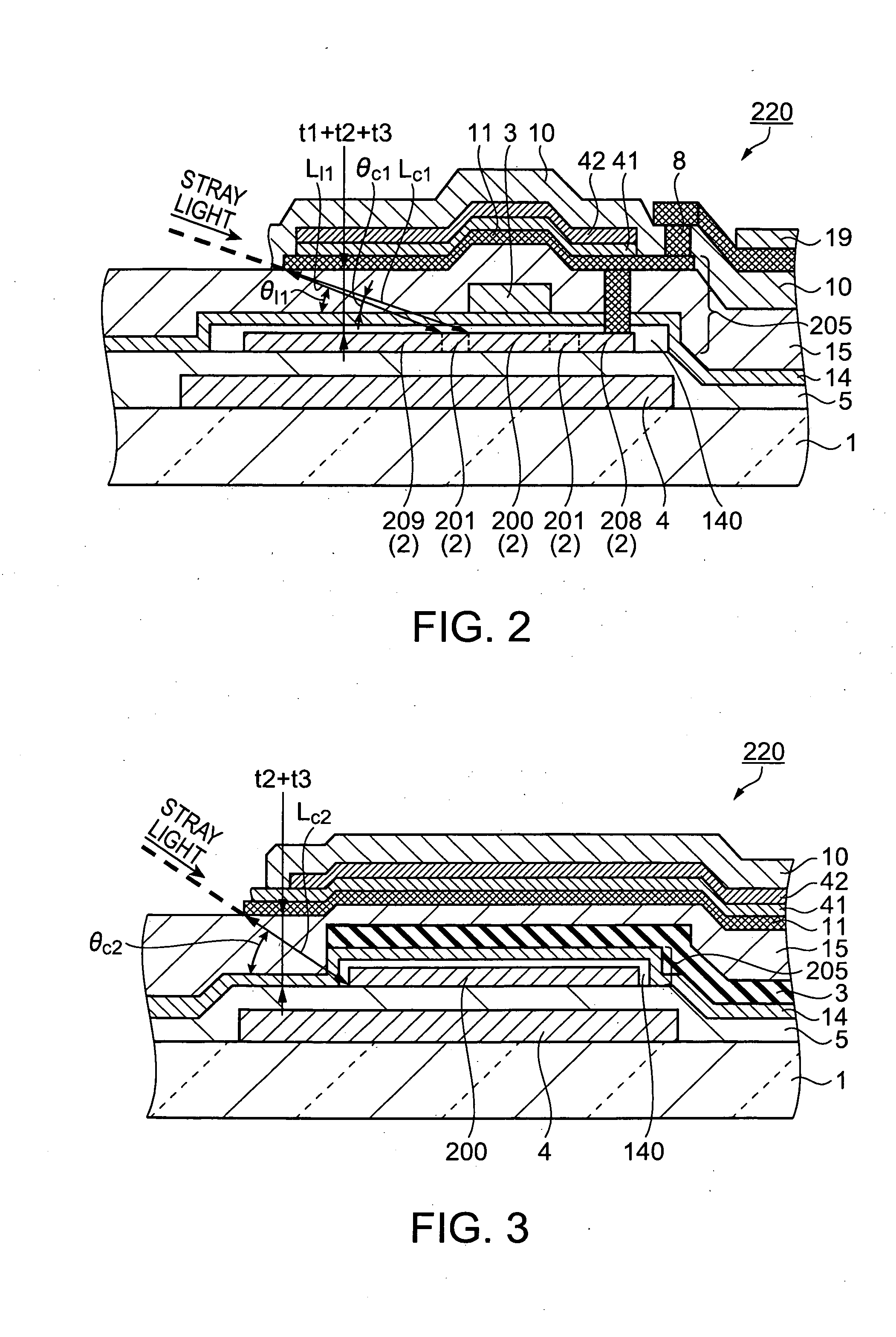
[0067]FIG. 12 is a view showing a state where the stray light penetrates into the channel region 200 of the thin-film transistor 205 at a penetration angle θc. To prevent the stray light from reaching the channel region 200, it is only necessary to set a layer-thickness t in a manner to fulfill the below expression based on the Rayleigh's diffraction condition.
tn×sin θc) (the relational expression 5a)
[0068]In the relational expression 5a, sin θc is set to opposite side / oblique side, and this relation can be expressed by the expr...
PUM
 Abstract
Description
Claims
Application Information
PatSnap Eureka turns technology decisions into work you can execute. Powered by our Innovation Knowledge Graph, it runs expert workflows across engineering, life sciences, materials and intellectual property. Get your review-ready output in minutes.


