Output stage and related logic control method applied to source driver/chip

a logic control and output stage technology, applied in logic circuits, pulse techniques, instruments, etc., can solve problems such as unsatisfactory integrity, unsatisfactory layout size, and adverse effects on the life span of transistors, so as to reduce the layout size of the polarization switching mechanism, improve the integrity of the source driver or source chip, and reduce the layout size of the mos transistor

Inactive Publication Date: 2008-11-27
FARADAY TECH CORP
View PDF3 Cites 10 Cited by
  • Summary
  • Abstract
  • Description
  • Claims
  • Application Information

AI Technical Summary

Benefits of technology

[0012]Due to a relative low swing range (e.g. voltage swing) of a negative polarization driving voltage, it has been enough to control polarization switching only through n-channel MOS transistors. There is no need of complete transmission gates for controlling polarization switch, which are required in the prior art. Likewise, due to a relative high swing range of a positive polarization driving voltage, it has been enough to control polarization switching only through p-channel MOS transistors, and no prior-art complete transmission gates are needed. Accordingly, the layout size of the polarization switching mechanism can be reduced while the integrity of the source driver or source chip can be improved.
[0013]In an embodiment, the first output circuit and the second output circuit are implemented based on an asymmetric device layout specification; and the first-type transistors and second-type transistors are implemented based on a symmetric device layout specification. According to an asymmetric device layout specification, the clearance between the source and gate of a MOS transistor and the clearance between the drain and gate of the MOS transistor are asymmetric or unequal. Such a design may reduce a layout size of the MOS transistor. If the clearance between the source and gate and the clearance between the drain and gate are symmetric or equal, the layout size is larger. Nevertheless, a larger layout size has a better resistance to high voltage and high current as well as electrostatic discharge (ESD). Therefore, it is desired to use transistors with asymmetric layouts in a front section of the output stage, but use transistors with symmetric layout in the last section of the polarization switching mechanism. In this way, a good balance between the layout size and the circuit integrity / durability can be achieved.
[0016]Another object of the present invention is to provide an output stage adapted to be used in a source chip or source driver. The output stage includes: at least one output circuit (e.g. the above-described first and / or second output circuits). Each output circuit has a corresponding output node, and provides a corresponding output signal at the corresponding output node according to a corresponding input signal. Each output circuit includes a stacking circuit, an output driver and at least one switching circuit. The stacking circuit outputs a corresponding signal from at least one front-stage output end according to the input signal; the output driver is coupled between the stacking circuit and the second output node, and having at least one driving input end corresponding to the front-stage output end of the stacking circuit; and each switching circuit is coupled between the front-stage output end and the corresponding driving input end. Each switching circuit conducts the front-stage output end coupled thereto to the corresponding driving input end so that the output driver selectively outputs the output signal (i.e. driving voltage) from the output node or connects the driving input end to a corresponding preset voltage (e.g. operational voltage) to provide high impedance at the output node. For performing polarization switching, the output stage is disposed with first-type transistors (e.g. n-channel MOS transistors) and second-type transistors (e.g. p-channel MOS transistors) to work with the first output circuit with a relative low swing input signal and the second output circuit with a relative high swing input signal. The output node of the first output circuit is coupled to the odd output channel and the even output channel via the first-type transistors so that the output node of the first output circuit is communicable with either of the odd output channel and the even output channel with or without the conduction of any of the second-type transistors; and the output node of the second output circuit is coupled to the odd output channel and the even output channel via the second-type transistors so that the output node of the second output circuit is communicable with either of the odd output channel and the even output channel with or without the conduction of any of the first-type transistors. In this way, the polarization inversion can be achieved.

Problems solved by technology

It is apparent that the layout size is undesirably large and the integrity is unsatisfactory.
Moreover, since the driving power in the output stage is of high voltage and high current, the life span of transistors might be adversely affected.
The resistance of transistors to electrostatic discharge (ESD) is also an issue to be carefully considered, particularly for the small transistors.

Method used


Image

  • Output stage and related logic control method applied to source driver/chip
  • Output stage and related logic control method applied to source driver/chip
  • Output stage and related logic control method applied to source driver/chip

Examples


Embodiment Construction

[0024]The present invention will now be described more specifically with reference to the following embodiments. It is to be noted that the following descriptions of preferred embodiments of this invention are presented herein for purpose of illustration and description only; it is not intended to be exhaustive or to be limited to the precise form disclosed.

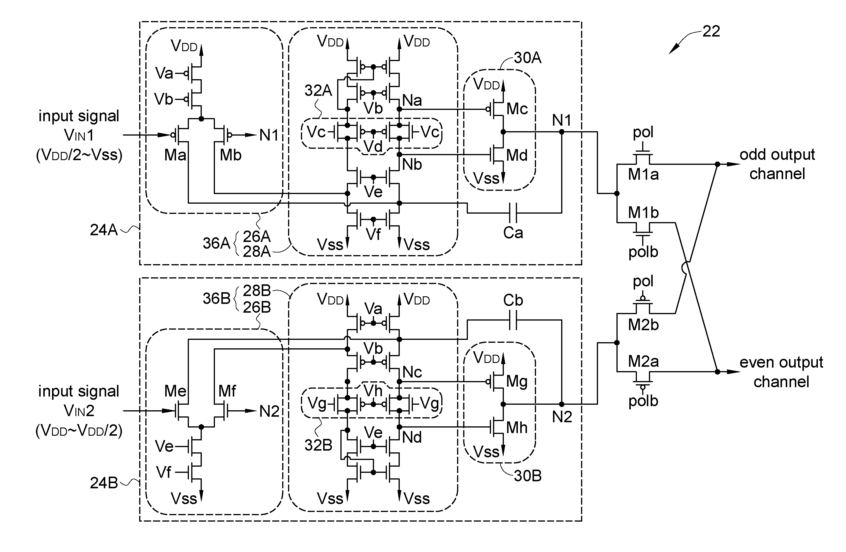
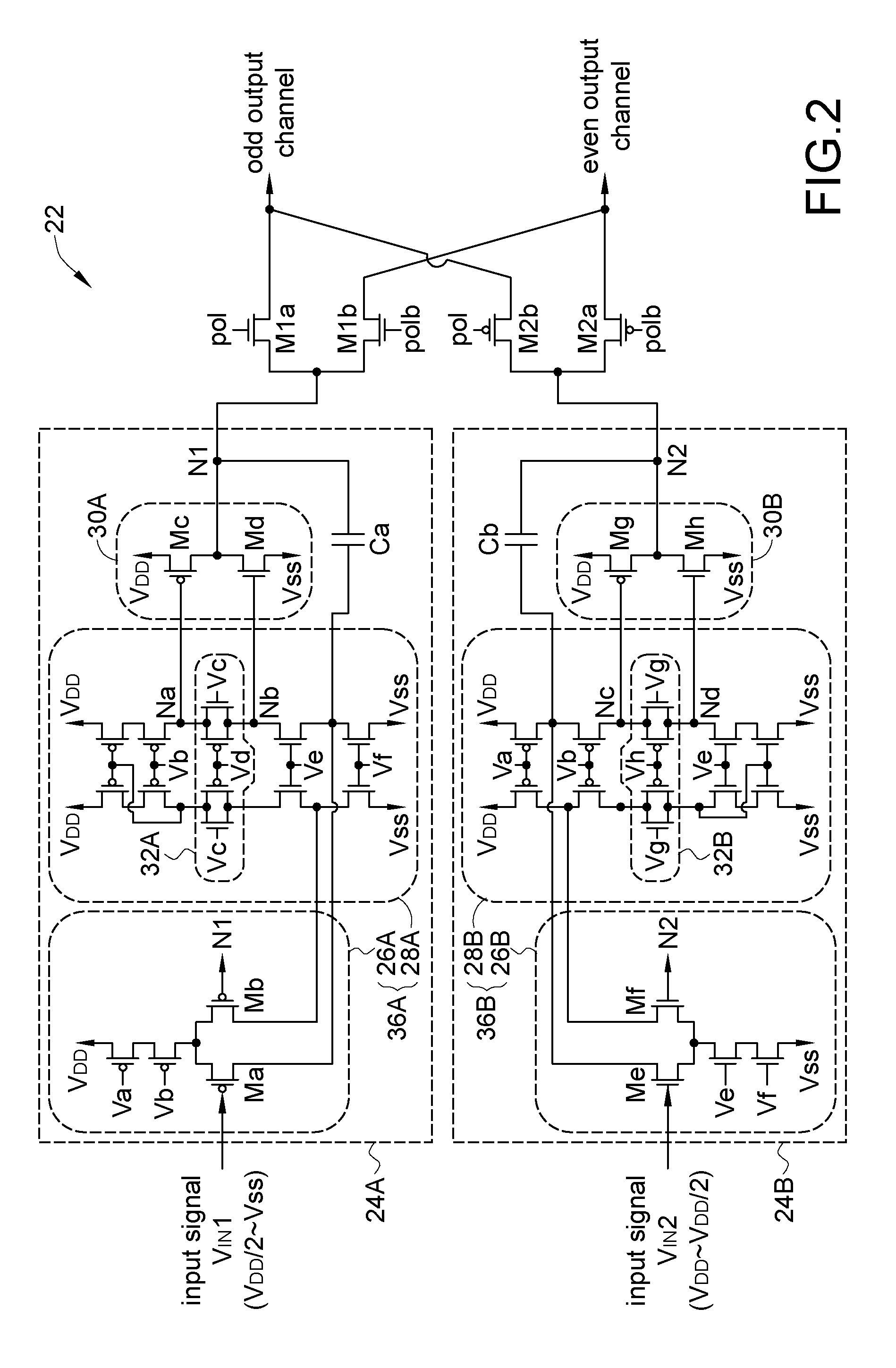
[0025]Please refer to FIG. 2, which illustrates circuitry of an embodiment of an output stage 22 according to the present invention. The output stage 22 is applicable to a source driver / chip such as a source chip of an LCD panel for source driving. As shown in FIG. 2, the output stage 22 is biased between operational voltages VDD and VSS and includes first and second output circuits 24A and 24B. The output circuit 24A receives an input signal VIN1 within a low swing range, e.g. a range between VDD / 2 and VSS, and drives to generate a negative polarization output signal at an output node N1 with a negative polarization driving volt...


PUM


Abstract

Output stage and related method applied to source driver / chip of LCD panel. While performing dot polarization inversion for even / odd channels of LCD panel, n-channel and p-channel MOS transistors of symmetric layout are respectively adopted for alternately transmitting a positive polarization signal of higher swing range and a negative polarization signal of lower swing range from corresponding drivers of asymmetric layout to the even / odd channels, such that a layout area for alternating polarizations can be reduced. Also, the invention directly ties inputs of the output drivers to VDD or VSS so as to turn off the drivers for providing high impedance at the even / odd channels when necessary.

Description

FIELD OF THE INVENTION[0001]The present invention relates to an output stage and a related method for use in a source driver / chip of an LCD panel, and more particularly to an output stage and a related method which use only n-channel / p-channel MOS transistors for alternately transmitting negative / positive polarization driving inputs in a dot polarization inversion mechanism, such that a layout area can be reduced, and turn off the output driving circuit for providing high impedance when necessary.BACKGROUND OF THE INVENTION[0002]A liquid crystal display (LCD) has become one of the most popular displaying devices nowadays. Thus circuits and means for driving LCD panels are one of the key techniques to be researched and developed in modern electronic industry. Give a thin-film transistor LCD (TFT-LCD) panel for example. A TFT-LCD panel generally includes a plurality of pixel units arranged in an array; and each TFT-LCD pixel unit typically includes a thin-film transistor and a LC ligh...

Claims


Application Information

Patent Timeline
Patent Type & Authority Applications(United States)
IPC IPC(8): H02H11/00H03K19/094
CPCG09G3/3614G09G3/3688G09G2310/0297
Inventor YANG, CHENG-YONG
Owner FARADAY TECH CORP
Why Eureka
Try Eureka