Nitride semiconductor light emitting device and method of fabricating nitride semiconductor laser device

a light emitting device and laser device technology, applied in the direction of semiconductor lasers, vacuum evaporation coatings, coatings, etc., can solve the problems of deformation of the facet, excessive heat generation of the facet, and impaired reliability of the semiconductor laser devi

Active Publication Date: 2008-11-27
SHARP FUKUYAMA LASER CO LTD
View PDF50 Cites 245 Cited by
  • Summary
  • Abstract
  • Description
  • Claims
  • Application Information

AI Technical Summary

Benefits of technology

[0008]The present inventors have studied to develop a technique to form a coating film of AlN aforementioned on a facet of a cavity to implement a nitride semiconductor laser device that can be driven for high output without impairing reliability as the cavity has the facet degraded.
[0028]The present invention can thus provide a nitride semiconductor light emitting device that can provide an improved COD level while it is aged, and a method of fabricating a nitride semiconductor laser device.

Problems solved by technology

It is generally known that a semiconductor laser device having a cavity with a facet degraded is impaired in reliability.
It is considered that a cavity has a facet degraded when a nonradiative recombination level exists and accordingly the facet excessively generates heat.
A major cause of such level is that the cavity has a facet oxidized.
A coating film which does not contain oxygen, however, is generally high in stress and considered to lead to degradation such as dark line for example.

Method used


Image

  • Nitride semiconductor light emitting device and method of fabricating nitride semiconductor laser device
  • Nitride semiconductor light emitting device and method of fabricating nitride semiconductor laser device
  • Nitride semiconductor light emitting device and method of fabricating nitride semiconductor laser device

Examples


first embodiment

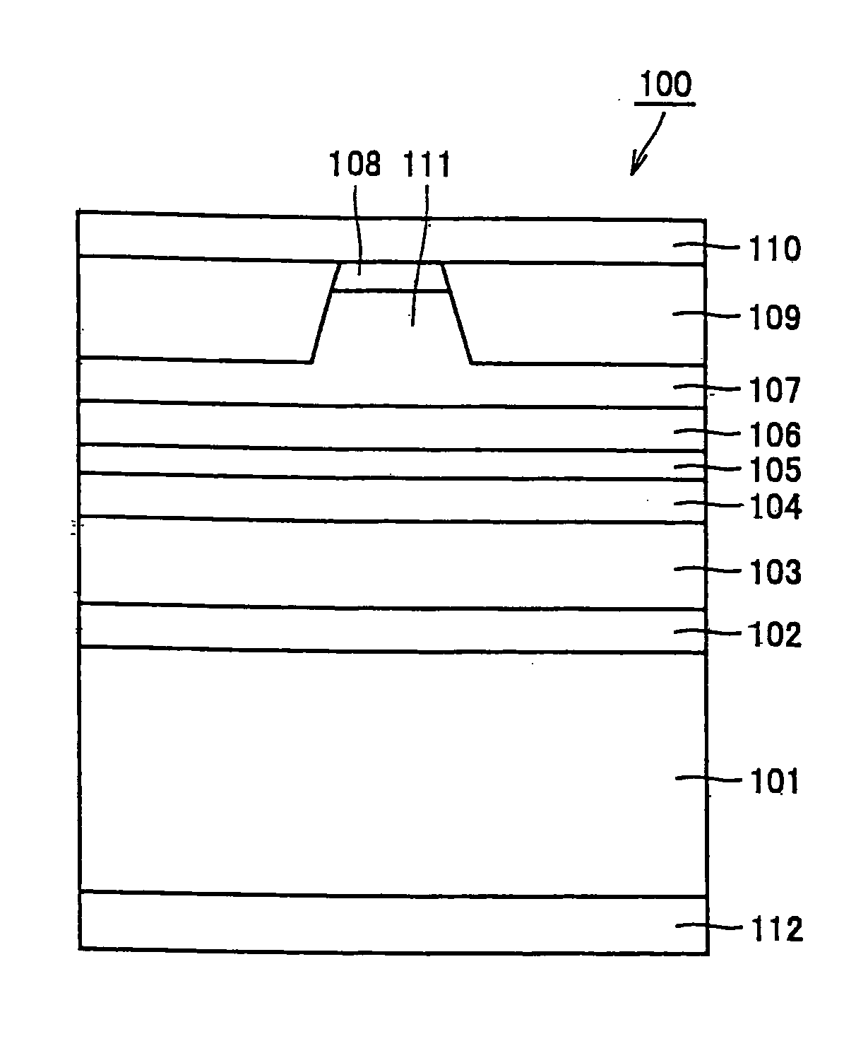
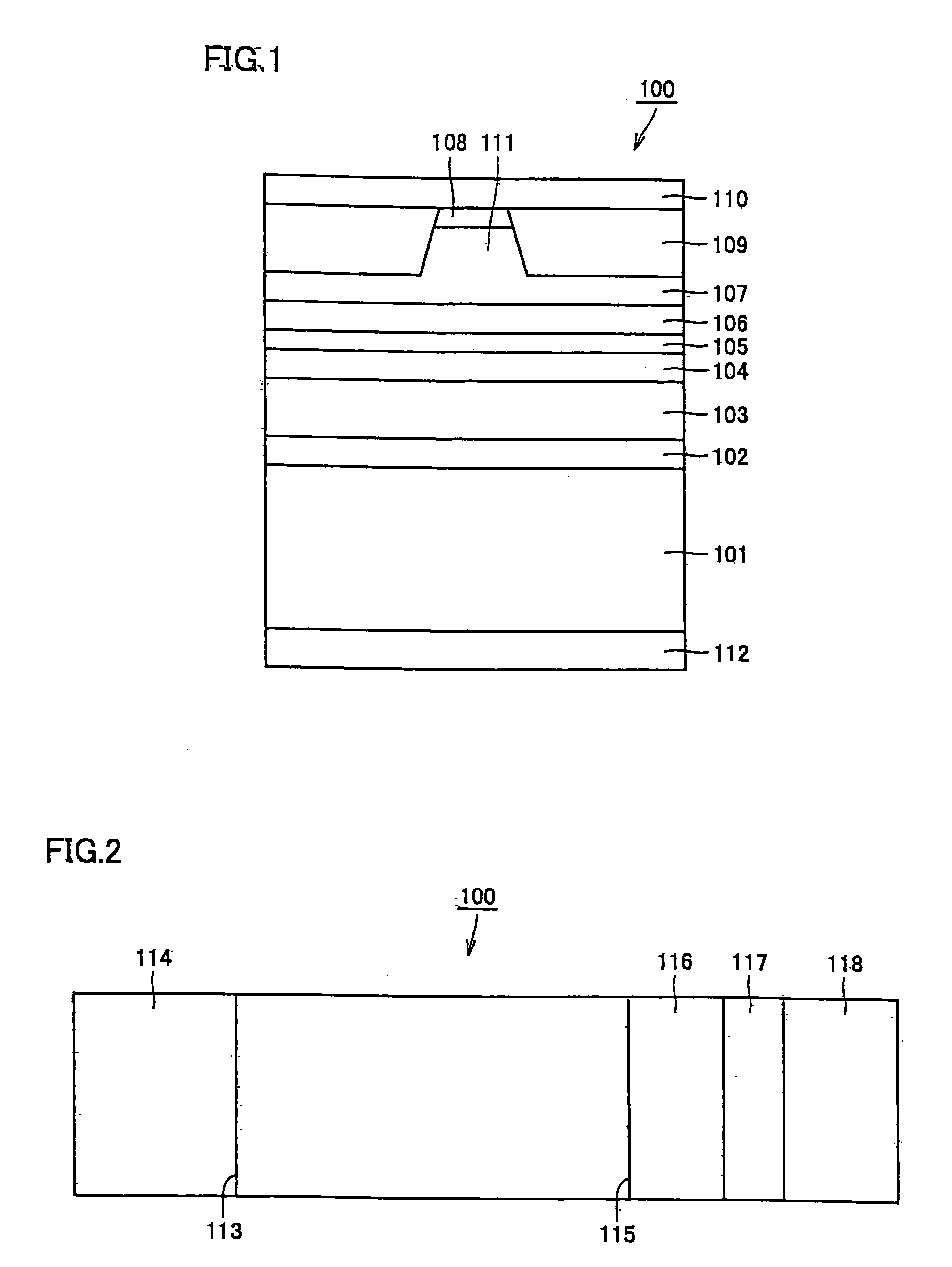
[0059]FIG. 1 is a schematic cross section of one preferred example of a nitride semiconductor laser device of the present embodiment. More specifically, the present embodiment provides a nitride semiconductor laser device 100 including an n type GaN substrate 101, an n type AlGaInN buffer layer 102 deposited thereon, an n type AlGaInN clad layer 103 deposited thereon, an n type AlGaInN guide layer 104 deposited thereon, an AlGaInN multi quantum well active layer 105 deposited thereon, a p type AlGaInN guide layer 106 deposited thereon, a p type AlGaInN clad layer 107 deposited thereon, and a p type AlGaInN contact layer 108 deposited thereon. It should be noted that each layer has a composition ratio adjusted as appropriate and thus irrelevant to the essence of the present invention. Furthermore in the present embodiment the nitride semiconductor laser device lases at a wavelength which can be adjusted, as appropriate, within a range for example of 370 nm to 470 nm depending on the ...

second embodiment

[0081]The present embodiment provides a nitride semiconductor laser device similar in configuration to that of the first embodiment except that the former has a cavity with a light emitting facet coated with a coating film modified in configuration and a light reflecting facet provided with a film modified in configuration.

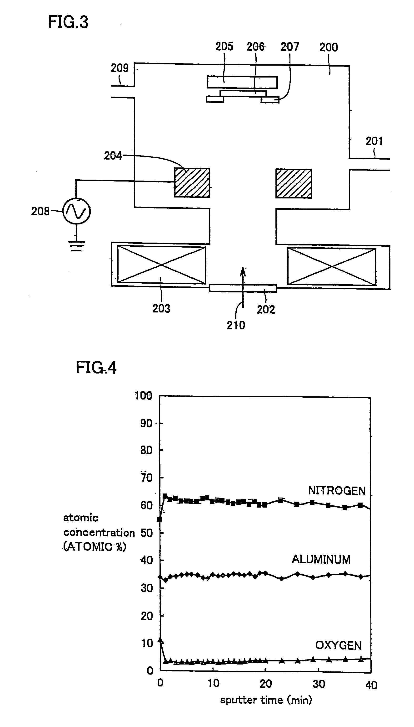
[0082]More specifically in the present embodiment the nitride semiconductor laser device has a cavity with a light emitting facet provided with a coating film formed of aluminum oxynitride and having a thickness of 6 nm. Furthermore the cavity has a light reflecting facet provided with a 12 nm thick aluminum oxynitride film deposited under the same conditions as the coating film coating the light emitting facet of the cavity and on the aluminum oxynitride film a 81 nm thick silicon oxide film and a 54 nm thick titanium oxide film serving as one pair are deposited by four pairs in layers, with the silicon oxide film first deposited, and thereafter on a frontmost su...

third embodiment

[0085]The present embodiment provides a nitride semiconductor laser device similar in configuration to that of the first embodiment except that the former has a cavity with a light emitting facet coated with a coating film modified in configuration and a light reflecting facet provided with a film modified in configuration.

[0086]More specifically in the present embodiment the nitride semiconductor laser device has a cavity with a light emitting facet provided with a coating film formed of aluminum oxynitride and having a thickness of 100 nm. Furthermore the cavity has a light reflecting facet provided with a 20 nm thick aluminum oxynitride film deposited under the same conditions as the coating film coating the light emitting facet of the cavity and on the aluminum oxynitride film a 81 nm thick silicon oxide film and a 54 nm thick titanium oxide film serving as one pair are deposited by four pairs in layers, with the silicon oxide film first deposited, and thereafter on a frontmost ...


PUM

PropertyMeasurementUnit
thickaaaaaaaaaa
reflectanceaaaaaaaaaa
thicknessaaaaaaaaaa

Abstract

There is provided a nitride semiconductor light emitting device having a light emitting portion coated with a coating film, the light emitting portion being formed of a nitride semiconductor, the coating film in contact with the light emitting portion being formed of an oxynitride. There is also provided a method of fabricating a nitride semiconductor laser device having a cavity with a facet coated with a coating film, including the steps of: providing cleavage to form the facet of the cavity; and coating the facet of the cavity with a coating film formed of an oxynitride.

Description

[0001]This nonprovisional application is based on Japanese Patent Application No. 2005-363590 filed with the Japan Patent Office on Dec. 16, 2005, the entire contents of which are hereby incorporated by reference.BACKGROUND OF THE INVENTION[0002]1. Field of the Invention[0003]The present invention relates to nitride semiconductor light emitting devices and methods of fabricating nitride semiconductor laser devices.[0004]2. Description of the Background Art[0005]It is generally known that a semiconductor laser device having a cavity with a facet degraded is impaired in reliability. It is considered that a cavity has a facet degraded when a nonradiative recombination level exists and accordingly the facet excessively generates heat. A major cause of such level is that the cavity has a facet oxidized.[0006]Accordingly Japanese Patent Laying-Open No. 09-162496 (Patent Document 1) discloses a method coating a facet of a cavity with a coating film formed of a nitride not excluding oxygen ...

Claims


Application Information

Patent Timeline
Patent Type & Authority Applications(United States)
IPC IPC(8): H01S5/323H01L33/00C23C14/06H01L21/318H01S5/343
CPCB82Y20/00H01L33/44H01S5/028H01S5/2036H01S5/22H01S5/34333H01S5/00
Inventor KAMIKAWA, TAKESHIKAWAGUCHI, YOSHINOBU
Owner SHARP FUKUYAMA LASER CO LTD
Why Eureka
Try Eureka