Deep anisotropic silicon etch method

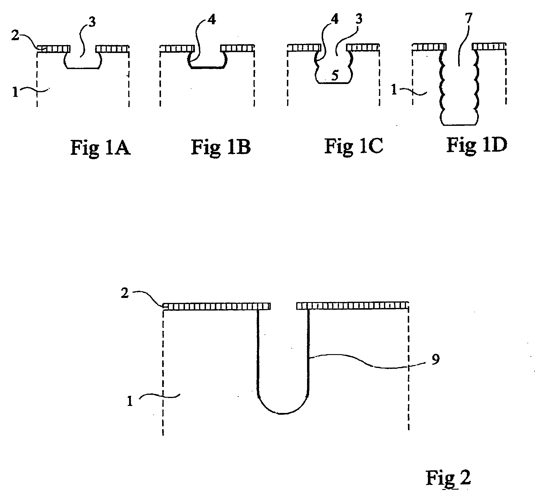
a silicon wafer and anisotropic technology, applied in the field of deep anisotropic etching of silicon wafers, can solve the problems of forming a polymer on the recess walls, the trench or the rib is grooved, and the walls of the obtained well are eroded,

Active Publication Date: 2008-11-27
STMICROELECTRONICS SRL +2
View PDF5 Cites 15 Cited by
  • Summary
  • Abstract
  • Description
  • Claims
  • Application Information

AI Technical Summary

Benefits of technology

[0023]Thus, a feature of the present invention is to provide a novel silicon plasma etch method which e...

Problems solved by technology

A disadvantage of the structure obtained by the alternated method is that the walls of the obtained well, trench or rib are grooved while they are smooth with the cryogenic method.
Another disadvantage of the alternated method with respect to the cryogenic method lies in the forming of a polymer on the recess walls.
This polymer is difficult to remove, which makes the method poorly adapted to certain applications in electronics where the quality of the contact with the trench walls is particularly important.
This polymer not only deposits in the formed recess but also on the reactor walls, which obliges to frequently cleaning this reactor and causes an efficiency decrease and method drifts.
Another disadvantage of the alternated method lies in the fact that, in given ...

Method used


Image

  • Deep anisotropic silicon etch method
  • Deep anisotropic silicon etch method
  • Deep anisotropic silicon etch method

Examples


example

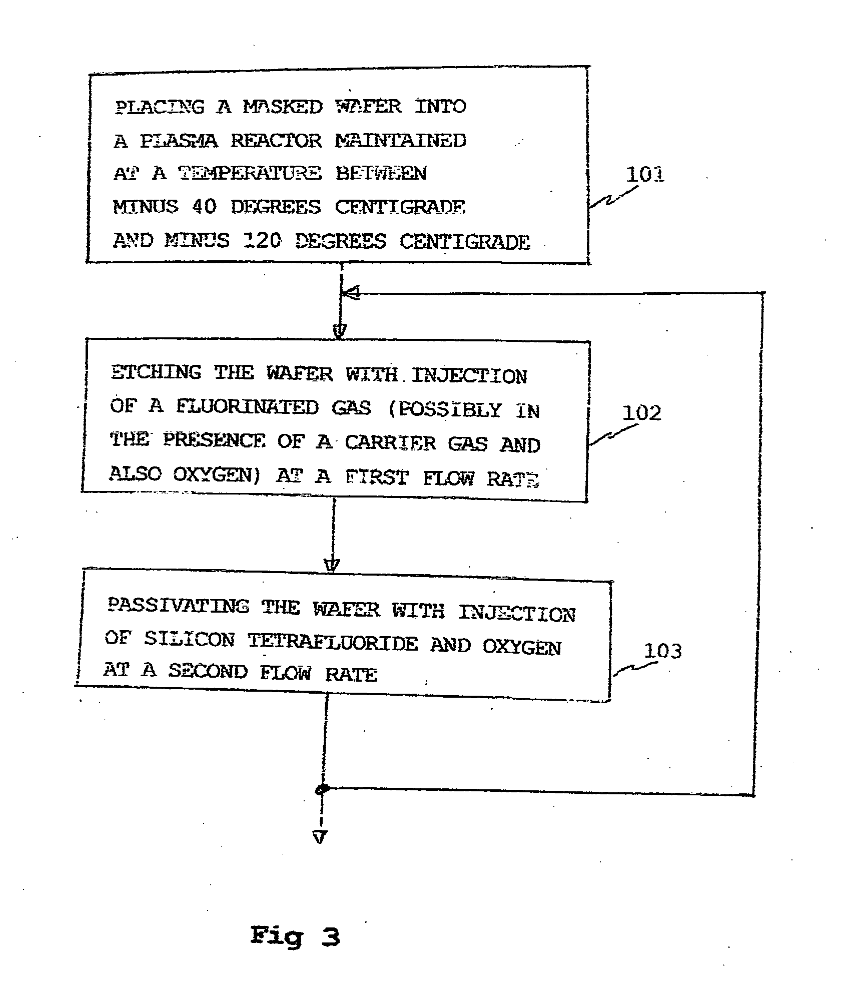
[0050]It may for example be worked in the following conditions:

[0051]etching: SF6 flow rate: 200 standard cm3 per minute (sccm) with a possible addition of 13 sccm Of O2,

[0052]passivation: SiF4 flow rate: 20 sccm and O2 flow rate 13 sccm,

[0053]in both cases, plasma conditions:

[0054]pressure: 3 Pa,

[0055]RF source power: 1000 W,

[0056]biasing: −60 V.

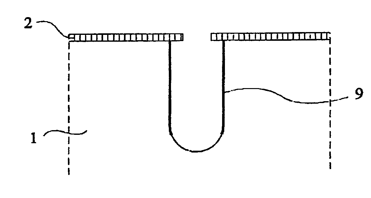
[0057]Under such conditions, an etch rate of 6 μm per minute is obtained in a trench having a 10-μm opening.

[0058]More generally, during the etching, the proportion between oxygen and sulfur hexafluoride may be on the order of from 5 to 10%. During the passivation steps, the proportion between oxygen and silicon tetrafluoride may be on the order of from 50 to 80%.

[0059]The SF6 flow rate for example ranges between 100 and 1000 sccm, preferably between 200 and 400 sccm. The SiF4 flow rate for example ranges between 5 and 50 sccm, preferably close to 20 sccm. The 02 flow rate for example ranges between 5 and 100 sccm, preferably between 10 and...


PUM

PropertyMeasurementUnit
Temperatureaaaaaaaaaa

Abstract

A method of anisotropic plasma etching of a silicon wafer, maintained at a temperature from −40° C. to −120° C., comprising alternated and repeated steps of:
    • etching with injection of a fluorinated gas, into the plasma reactor, and
    • passivation with injection of silicon tetrafluoride, SiF4, and of oxygen into the plasma reactor, the flow rate of the gases in the plasma reactor being on the order of from 10% to 25% of the gas flow rate during the etch step.

Description

BACKGROUND OF THE INVENTION[0001]1. Field of the Invention[0002]The present invention relates to the field of microcomponents and Microsystems, and more specifically to methods of deep anisotropic etching of a silicon wafer.[0003]2. Discussion of the Related Art[0004]Two main methods for anisotropically etching wells, trenches or ribs (mesas) in silicon wafers are industrially used.[0005]A first so-called alternated method is for example described in U.S. Pat. No. 5,501,893 of Bosch Company.[0006]As illustrated in FIGS. 1A to 1D, the alternated method comprises a repeated succession of etch and polymerization steps which are implemented at a temperature close to the ambient temperature.[0007]FIG. 1A is a partial view of a silicon wafer 1 coated with a protection layer 2, for example, a silicon oxide layer in which an opening 3 has been formed, for example, a circular hole or a strip of small width. The silicon wafer is placed in a plasma reactor (not shown) and a first recess 3 is e...

Claims


Application Information

Patent Timeline
IPC IPC(8): H01L21/3065
CPCB81B2203/033B81C2201/0112H01L21/30655B81C1/00619
Inventor DUSSART, REMILEFAUCHEUX, PHILIPPEMELLIHAOUI, XAVIEROVERZET, LAWRENCE JOHNRANSON, PIERRETILLOCHER, THOMASBOUFNICHEL, MOHAMED
Owner STMICROELECTRONICS SRL
Why Eureka
Try Eureka