Slew constrained minimum cost buffering

a buffering and minimum cost technology, applied in the direction of cad circuit design, program control, instruments, etc., can solve the problems of large number of cells, difficult to achieve physical design without the aid of computers, and require complicated connections between cells, so as to maintain legal slew constraints and reduce or minimize the buffer cost (area)

Inactive Publication Date: 2008-11-27
GLOBALFOUNDRIES INC
View PDF4 Cites 1 Cited by
  • Summary
  • Abstract
  • Description
  • Claims
  • Application Information

AI Technical Summary

Benefits of technology

[0017]It is another object of the present invention to provide such a method which reduces or minimizes the buffer cost (area) while maintaining legal slew constraints.
[0018]It is yet another object of the present invention to provide a method and system for buffer insertion which is efficient in the presence of blockages and handling of multi-fanout nets.

Problems solved by technology

An IC may include a very large number of cells and require complicated connections between the cells.
Due to the large number of components and the details required by the fabrication process for very large scale integrated (VLSI) devices, physical design is not practical without the aid of computers.
As process technology scales to the submicron regime, interconnect delays increasingly dominate gate delays.
Therefore, both the complexity and importance of buffer insertion is increasing in an even faster pace.
However, physical synthesis can take days to complete.
Increasing the frequency of buffer insertion locations can improve timing of the net, but at an increased buffer cost, i.e., an increased size or area of the silicon chip used for the buffers.
While this approach provides a valuable tool for delay optimization, it does not address other important electrical characteristics such as slew.
Since higher interconnect resistivity also causes signal integrity to degrade more quickly with each advancing technology, buffers need to be inserted on long interconnects to meet slew constraints.
This large number of buffers can degrade overall design performance by forcing the rest of the logic to be spread further apart to accommodate the buffers.
The buffers themselves are a drain on power and can cause other gates to be sized to higher power levels since they are further apart on the chip.
Prior art buffer insertion tools fail to adequately deal with slew constraints as they pertain to the increased costs from buffering.
However, that approach merely integrates slew constraints while still optimizing for delay, and buffering of non-critical nets may result in unnecessary runtime and resource overhead.
Other approaches have different limitations.
189-194 (2001), tries to reduce buffer and wire congestion but it can be area inefficient especially in the presence of blockages and its handling of multi-fanout nets.
408-415 (2001), addresses slew constraints without regard to delay; however that technique does not model slew, it just simplifies the slew constraint to be equivalent to a capacitance constraint, so interconnected resistivity is not actually modeled.

Method used


Image

  • Slew constrained minimum cost buffering
  • Slew constrained minimum cost buffering
  • Slew constrained minimum cost buffering

Examples


Embodiment Construction

)

[0029]The present invention provides a novel method for determining buffer insertion locations in a net of an integrated circuit design, and is generally applicable to any type of IC design, such as general-purpose microprocessors, memory units or special-purpose circuitry. The method may be implemented as part of a physical synthesis process which optimizes placement, timing, power consumption, crosstalk effects or other design parameters. As explained more fully below, an exemplary embodiment of the present invention provides a fast technique which can handle a large volume of nets to optimally solve slew buffering while also reducing buffering cost.

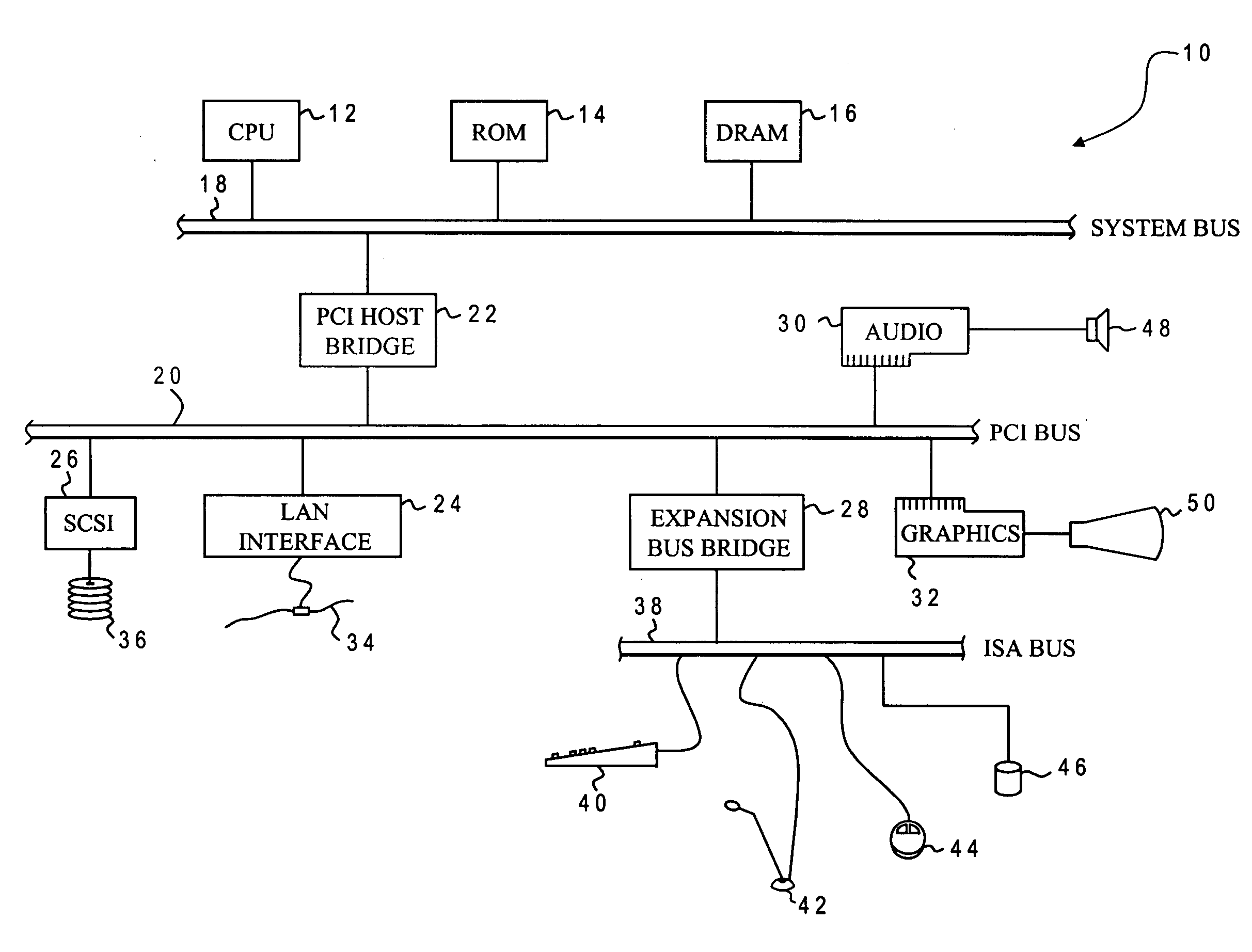
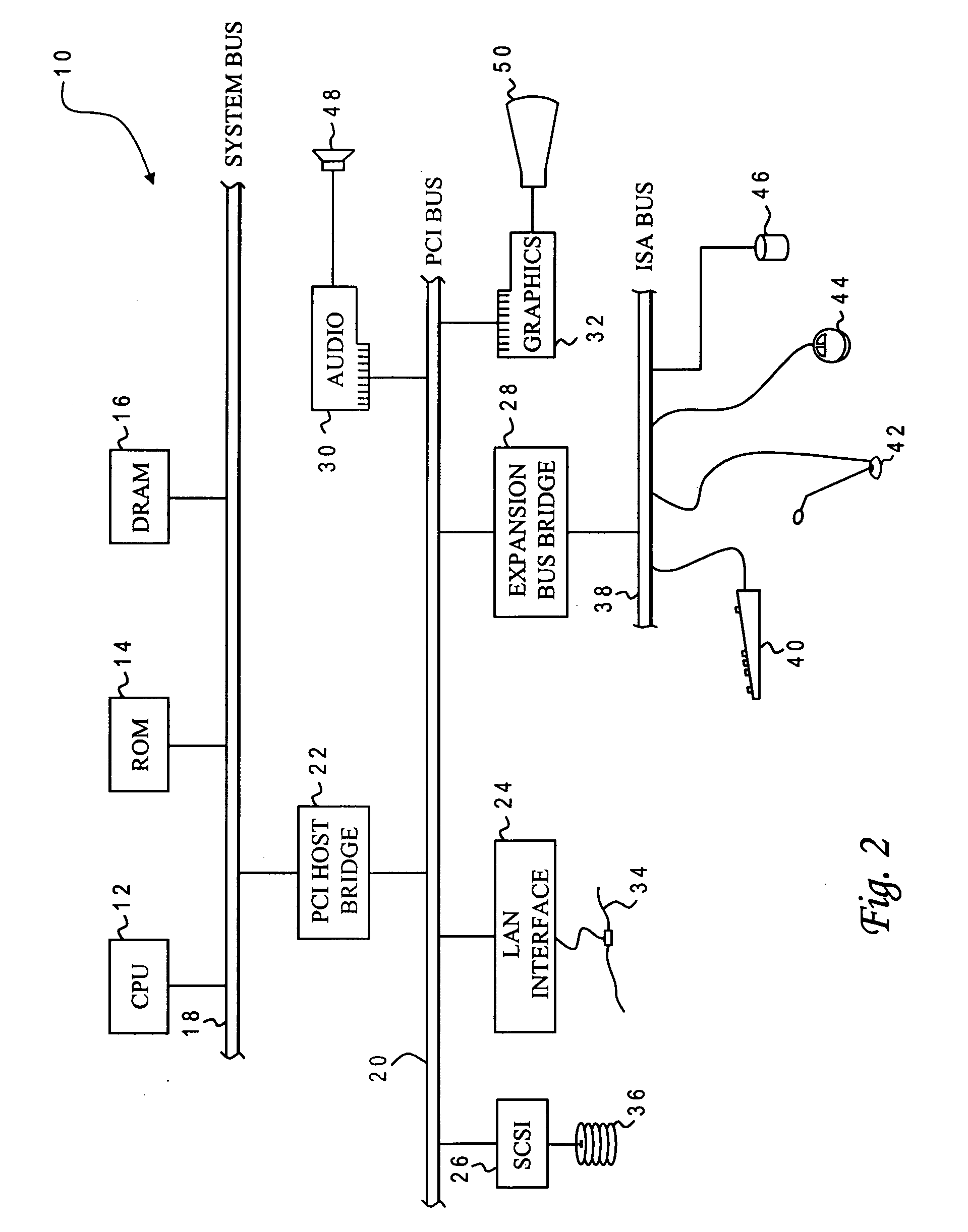
[0030]With reference now to the figures, and in particular with reference to FIG. 2, there is depicted one embodiment 10 of a computer system programmed to carry out the buffer insertion in accordance with one implementation of the present invention. System 10 includes a central processing unit (CPU) 12 which carries out program instr...


PUM


Abstract

A buffer insertion technique addresses slew constraints while minimizing buffer cost. The method builds initial solutions for the sinks, each having an associated cost, slew and capacitance. As a solution propagates toward a source, wire capacitance and wire slew are added to the solution. When a buffer is selected for possible insertion, the slew of the solution is set to zero while the cost of the solution is incremented based on the selected buffer and the capacitance is set to an intrinsic capacitance of the buffer. The solutions of two intersecting wire branches are merged by adding branch capacitances and costs, and selecting the highest branch slew. The solution sets are updated by disregarding solutions which have a slew component greater than a slew constraint, and any solution that is dominated by another solution is eliminated. The solution having the smallest cost is selected as the final solution.

Description

CROSS-REFERENCE TO RELATED APPLICATION[0001]This application is a continuation of U.S. patent application Ser. No. 11 / 457,495 filed Jul. 14, 2006.BACKGROUND OF THE INVENTION[0002]1. Field of the Invention[0003]The present invention generally relates to the design of semiconductor chips and integrated circuits, and more particularly to the use of buffer insertion to manage timing and electrical requirements in an integrated circuit design.[0004]2. Description of the Related Art[0005]Integrated circuits are used for a wide variety of electronic applications, from simple devices such as wristwatches, to the most complex computer systems. A microelectronic integrated circuit (IC) chip can generally be thought of as a collection of logic cells with electrical interconnections between the cells, formed on a semiconductor substrate (e.g., silicon). An IC may include a very large number of cells and require complicated connections between the cells. A cell is a group of one or more circuit ...

Claims


Application Information

Patent Timeline
Patent Type & Authority Applications(United States)
IPC IPC(8): G06F17/50
CPCG06F17/5045G06F30/30
Inventor ALPERT, CHARLES J.KARANDIKAR, ARVIND K.MAHMUD, TUHINQUAY, STEPHEN T.SZE, CHIN NGAI
Owner GLOBALFOUNDRIES INC
Why Eureka
Try Eureka