Programmable semiconductor interposer for electronic package and method of forming

a technology of semiconductor interposers and electronic packages, which is applied in the direction of semiconductor devices, semiconductor/solid-state device details, electrical apparatus, etc., can solve the problems of low thermal expansion efficiency of package substrates, solder bumps and dies that cannot be ripped off of packages, and relatively large die area occupied by hard-to-scale circuits, etc., to achieve the effect of reducing the cost and cycle time of integrated circuit products

Active Publication Date: 2008-12-04
TAIWAN SEMICON MFG CO LTD
View PDF25 Cites 114 Cited by
  • Summary
  • Abstract
  • Description
  • Claims
  • Application Information

AI Technical Summary

Benefits of technology

[0010]An advantage of preferred embodiments of the present invention is that devices formed in an interposer embodiment of the current invention can be selectively connected by a device selection unit to form a custom circuit function, which, in turn, can be coupled to an integrated circuit die.
[0011]A further advantage of a preferred embodiment of the present invention is that the initial design and manufacturing cost of an interposer can be shared by many different customers, which would preferably reduce the cost and cycle time of an integrated circuit product.

Problems solved by technology

In the meantime, forming a complex electronic system on an integrated circuit die results in the need for a large number of input / output (I / O) connections between an integrated circuit die and the rest of the electronic system of which the integrated circuit is a part.
Although flip-chip BGA packages provide a space-saving solution, other technical challenges remain to be addressed.
First, the coefficient of thermal expansion of a package substrate (in general, a dielectric material) does not provide a good match with the semiconductor material of an integrated circuit die.
Thermal stress could cause the solder bumps and die to tear free of the package, which casts a major reliability concern on the package of this configuration.
Second, for example, as the device feature sizes in the logical part of a system-on-chip integrated circuit continue to shrink, a relatively large portion of die area will be occupied by hard-to-scale circuits such as RF circuits, wherein large value capacitors and inductors are usually required for circuit function.
This phenomenon will eventually lead to a point where further scaling down of die size will become extremely difficult, if not impossible.
The other issue facing the SOC configuration is the increasing challenge on SOC design, where, for example, integrating digital and RF functions on a same die has made circuit modeling much more complicated and on-chip signal interference difficult to resolve.
This and other challenges have lead to the adoption of an interposer in an electronic package, where a structure made of material having a matching coefficient of thermal expansion to a semiconductor die is provided between an integrated circuit die and package substrate.
As an example, placing a decoupling capacitor into an integrated circuit die requires dramatic increase on die size, while placing it on a printed circuit board causes undesirable parasitic inductance associated with metal traces and package leads.
However, technical drawback remains in a prior art interposer.
Due to this nature, an electronic package involving a prior art interposer is in general very costly to design and manufacture.
In practice, only integrated circuit products of large market volume can justify the cost relating to the interposer containing package scheme.
This drawback has hindered prior art interposers from quicker and wider adoption in electronic packaging.

Method used


Image

  • Programmable semiconductor interposer for electronic package and method of forming
  • Programmable semiconductor interposer for electronic package and method of forming
  • Programmable semiconductor interposer for electronic package and method of forming

Examples


Embodiment Construction

[0027]The making and forming of the presently preferred embodiments are discussed in detail below. It should be appreciated, however, that the present invention provides many applicable inventive concepts that can be embodied in a wide variety of specific contexts. The specific embodiments discussed are merely illustrative of specific ways to make and use the invention, and do not limit the scope of the invention.

[0028]The present invention will be described with respect to preferred embodiments in a specific context, namely a standardized, user programmable silicon interposer structure with an array arrangement of passive and / or active devices, and the methods of forming the same. The invention also encompasses the structure and method of forming an electronic package comprising said interposer.

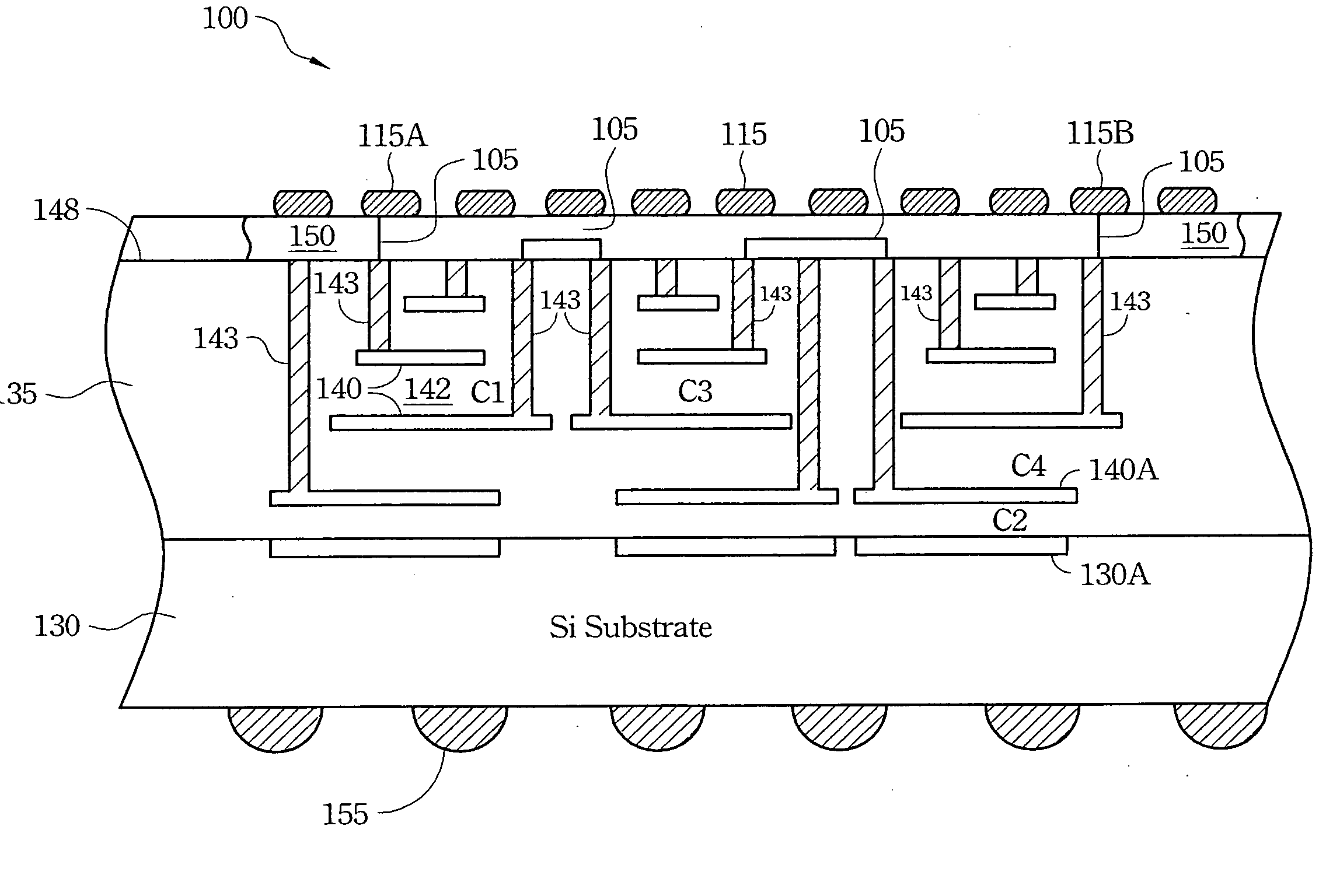
[0029]FIG. 3 is a schematic top view of one embodiment in accordance with the current invention, where the arrangement of passive devices in an interposer 100 is shown. Interposer 100 includ...


PUM


Abstract

Various structures of a programmable semiconductor interposer for electronic packaging are described. An array of semiconductor devices having various values is formed in said interposer. A user can program said interposer and form a “virtual” device having a desired value by selectively connecting various one of the array of devices to contact pads formed on the surface of said interposer. An inventive electronic package structure includes a standard interposer having an array of unconnected devices of various values and a device selection unit, which selectively connects various one of the array of devices in said standard interposer to an integrated circuit die encapsulated in said electronic package. Methods of forming said programmable semiconductor interposer and said electronic package are also illustrated.

Description

TECHNICAL FIELD[0001]The present invention relates generally to a semiconductor interposer in an electronic package and method of forming the same, and more particularly to a standard, programmable interposer wherein desired circuit functions can be formed and coupled to an integrated circuit die attached to said interposer.BACKGROUND[0002]As the trend to provide substantially increased circuit functionality on an integrated circuit die continues, the so-called system-on-chip (SOC) integrated circuit configuration has rapidly gained popularity in almost all application fields of an integrated circuit. It has hence become necessary to form a tremendously large number of transistors on an integrated circuit die. In the meantime, forming a complex electronic system on an integrated circuit die results in the need for a large number of input / output (I / O) connections between an integrated circuit die and the rest of the electronic system of which the integrated circuit is a part. New pac...

Claims


Application Information

Patent Timeline
Patent Type & Authority Applications(United States)
IPC IPC(8): H01L23/525
CPCH01L23/147H01L23/49827H01L2924/1305H01L2924/1461H01L21/76886H01L23/5382H01L23/642H01L23/645H01L2224/16H01L2924/01078H01L2924/10253H01L2924/15174H01L2924/15311H01L2924/19011H01L2924/13091H01L2924/15192H01L2924/00H01L2924/00014H01L25/0652H01L25/0655H01L25/0657H01L2224/13025H01L2224/16145H01L2224/16146H01L2224/16227H01L2224/16235H01L2224/17181H01L2225/06517H01L2225/06589H01L2924/157H01L2225/06513H01L2225/06541H01L2924/00011H01L2224/16225H01L2224/0401
Inventor HSU, CHAO-SHUNCHAO, CLINTONPENG, MARK SHANE
Owner TAIWAN SEMICON MFG CO LTD
Why Eureka
Try Eureka