Semiconductor substrate and manufacturing method of semiconductor device

a semiconductor and substrate technology, applied in semiconductor devices, semiconductor/solid-state device details, electrical devices, etc., can solve problems such as degradation of semiconductor elements characteristics, and achieve the effects of reducing gate leakage, suppressing crystal defects caused by strain stress, and improving withstand voltag

Inactive Publication Date: 2008-12-04
SEMICON ENERGY LAB CO LTD
View PDF15 Cites 28 Cited by
  • Summary
  • Abstract
  • Description
  • Claims
  • Application Information

AI Technical Summary

Benefits of technology

[0012]By providing a plurality of insulating layers having different functions between a supporting substrate and a single-crystal semiconductor layer, the supporting substrate and the single-crystal semiconductor layer formed of different materials are bonded. Furthermore, the single-crystal semiconductor layer can be prevented from being contaminated with impurities, and generation of crystal defects caused by application of strain stress can be suppressed. When the relief layer includes nitrogen at a concentration of 20 at. % or less and hydrogen (and / or an OH group) at a concentration of 0.1 at. % to 10 at. % to have structural flexibility, stress warping generated in the case where different materials are made in close contact with each other can be relieved efficiently. An insulating layer containing a halogen can capture metal impurities and prevent a single-crystal semiconductor layer from being contaminated.
[0013]When an insulating layer formed by a microwave plasma CVD method is used as an insulating layer (particularly, a gate insulating layer) of a semiconductor integrated circuit, the withstand voltage can be improved. Further, gate leakage can be reduced, and a semiconductor device having excellent hot carrier resistance can be provided.

Problems solved by technology

This generates a defect in the single-crystal semiconductor layer in some cases, which causes degradation of characteristics of the semiconductor element.

Method used


Image

  • Semiconductor substrate and manufacturing method of semiconductor device
  • Semiconductor substrate and manufacturing method of semiconductor device
  • Semiconductor substrate and manufacturing method of semiconductor device

Examples


Embodiment Construction

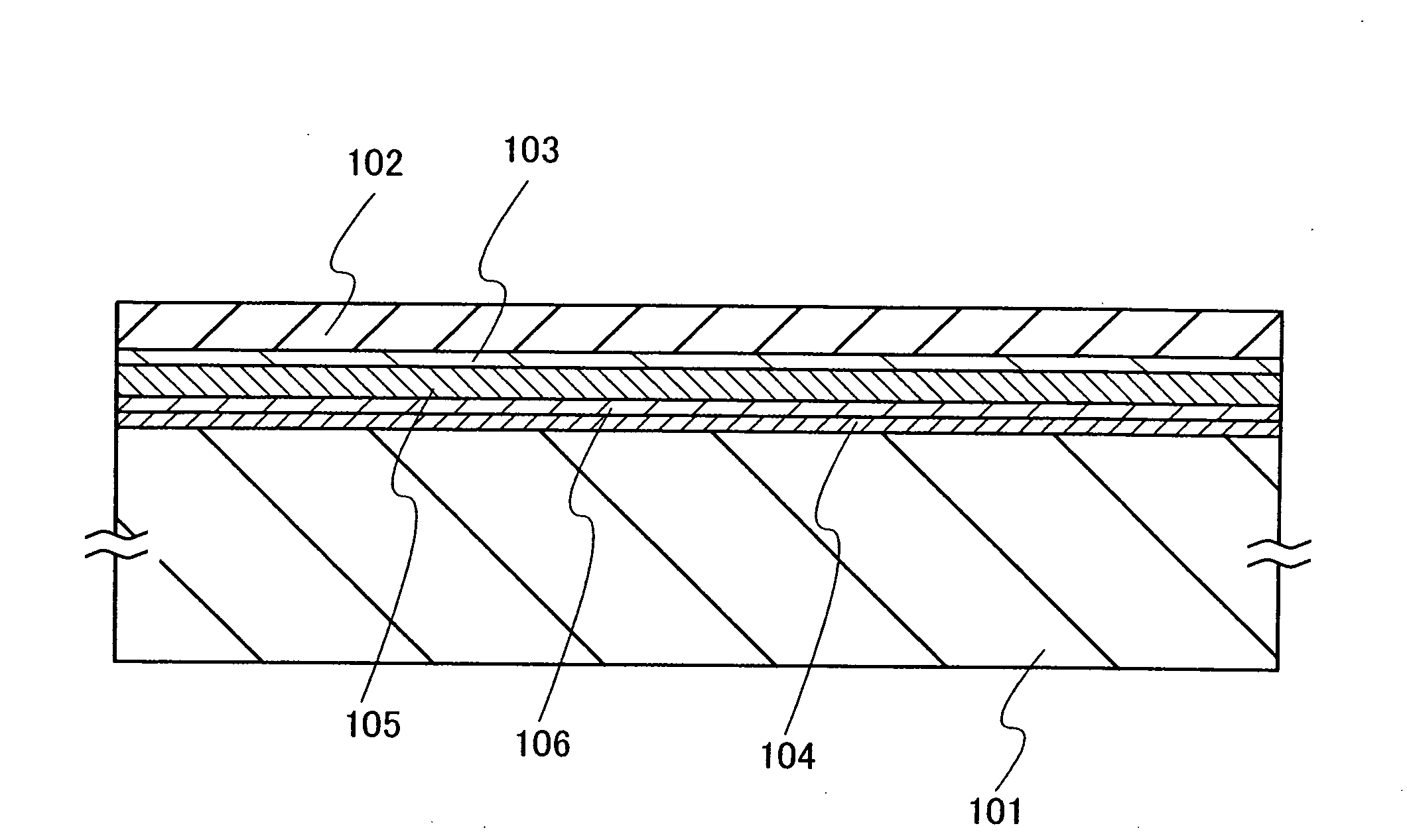
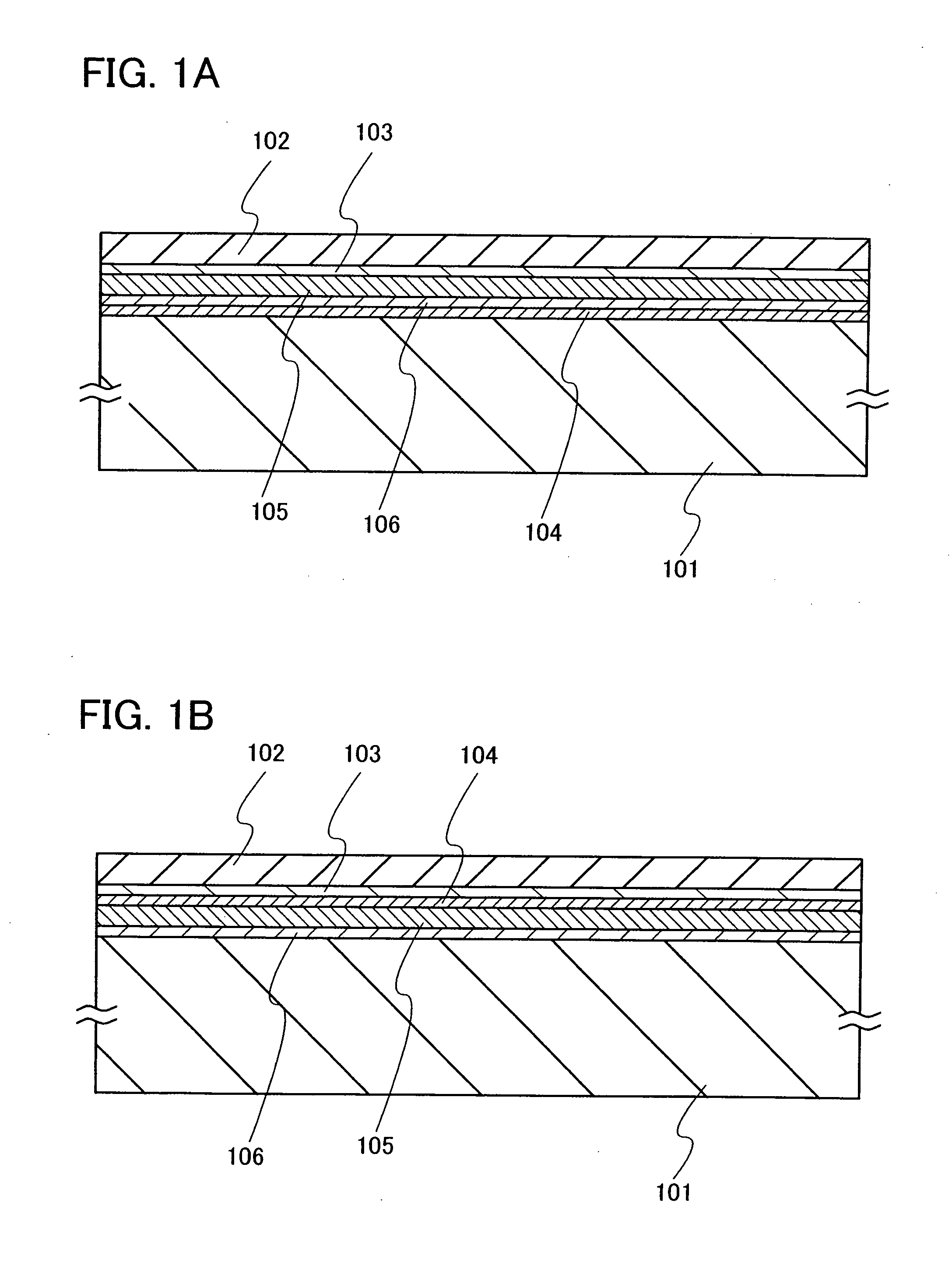
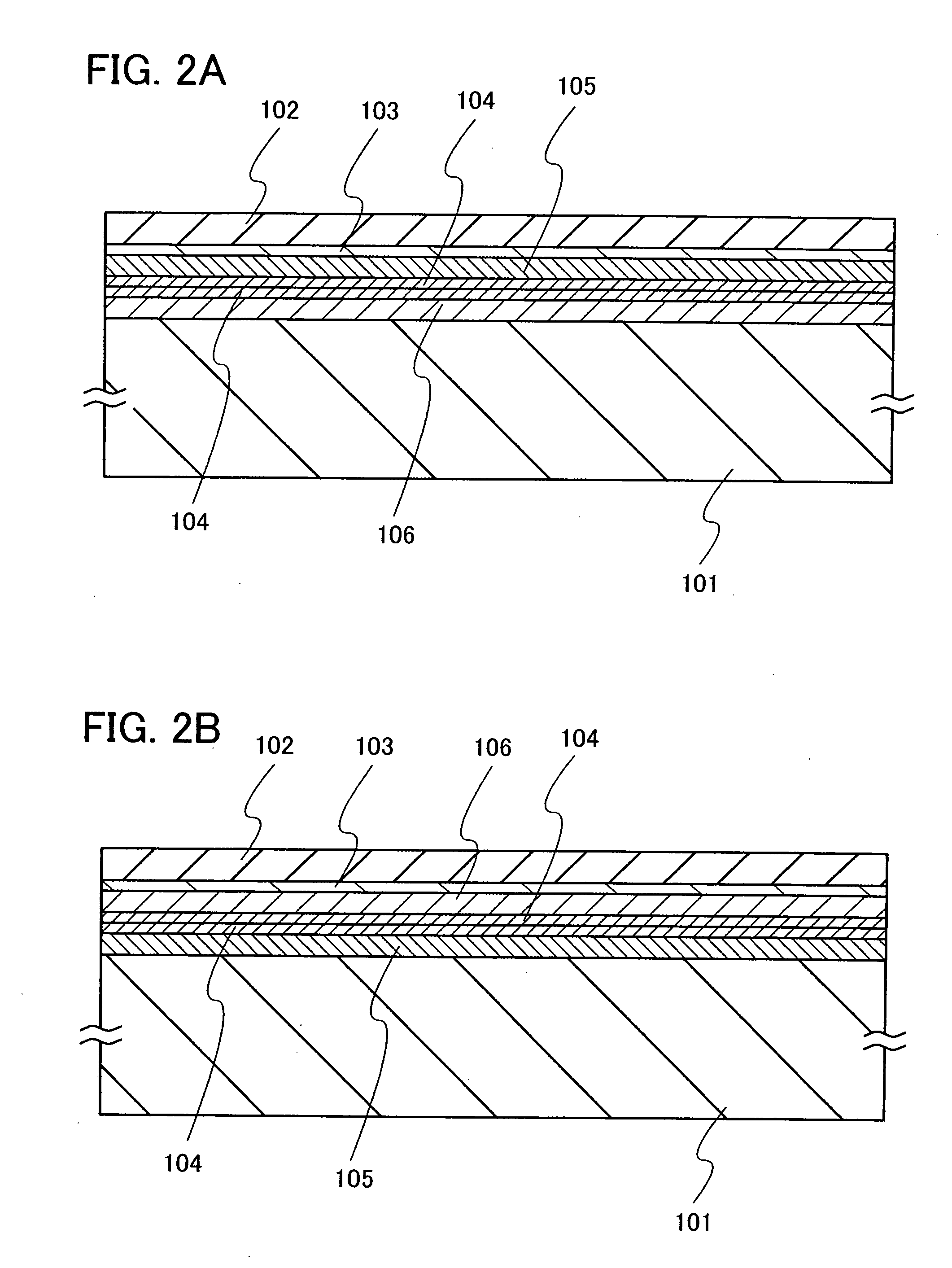
[0037]Embodiment Mode of the present invention will be described below with reference to the drawings. It is easily understood by those skilled in the art that various changes may be made in forms and details without departing from the spirit and the scope of the invention. Therefore, the present invention should not be interpreted as being limited to the descriptions of the embodiment mode below. In structures of the present invention described below, the same reference numerals are commonly given to the same components or components having similar functions throughout the drawings.

[0038]The cases where a single-crystal semiconductor layer is provided over a substrate having an insulating surface or an insulating substrate are described below; however, if a different kind of semiconductor substrate is used as a parent body of the semiconductor layer, a polycrystalline semiconductor layer can also be bonded to a substrate having an insulating surface or an insulating substrate.

[0039...


PUM

PropertyMeasurementUnit
strain pointaaaaaaaaaa

Abstract

To provide a semiconductor substrate including a crystalline semiconductor layer which is suitable for practical use, even if a material different from that of the semiconductor layer is used for a supporting substrate, and a semiconductor device using the semiconductor substrate. The semiconductor substrate includes a bonding layer which forms a bonding plane, a barrier layer formed of an insulating material containing nitrogen, a relief layer which is formed of an insulating material that includes nitrogen at less than 20 at. % and hydrogen at 1 at. % to 20 at. %, and an insulating layer containing a halogen, between a supporting substrate and a single-crystal semiconductor layer. The semiconductor device includes the above-described structure at least partially, and a gate insulating layer formed by a microwave plasma CVD method using SiH4 and N2O as source gases is in contact with the single-crystal semiconductor layer.

Description

BACKGROUND OF THE INVENTION[0001]1. Field of the Invention[0002]The present invention relates to a silicon-on-insulator (SOI) structure formed using a bonding technique, and particularly relates to a manufacturing method of a semiconductor substrate in which a single-crystal semiconductor layer is bonded to a supporting substrate which has an insulating surface, such as a glass substrate or the like. Further, the present invention relates to display devices and semiconductor devices formed using a semiconductor substrate having such an SOI structure, and a manufacturing method thereof.[0003]2. Description of the Related Art[0004]Semiconductor substrates called silicon-on-insulator (SOI substrate), in each of which a thin single-crystal semiconductor layer is formed on an insulating layer, have been developed instead of silicon wafers manufactured by thinly slicing single-crystal semiconductor ingots. In an integrated circuit using a semiconductor substrate, parasitic capacitance of ...

Claims


Application Information

Patent Timeline
Patent Type & Authority Applications(United States)
IPC IPC(8): H01L23/58H01L21/762
CPCH01L21/76254H01L21/84
Inventor YAMAZAKI, SHUNPEIICHIJO, MITSUHIROFURUNO, MAKOTOOHTSUKI, TAKASHIOKAZAKI, KENICHITANAKA, TETSUHIROYASUMOTO, SEIJI
Owner SEMICON ENERGY LAB CO LTD
Why Eureka
Try Eureka