Method for producing annealed wafer and annealed wafer

a technology of annealing and annealing wafers, which is applied in the direction of semiconductor/solid-state device manufacturing, basic electric elements, electric apparatus, etc., can solve the problems of inability to ignore the size of the grown-in defect, the resistivity of the wafer cannot be sure prevented from changing before and after heat treatment, and the effect of low-density grown-in defects

Active Publication Date: 2010-02-09
SHIN-ETSU HANDOTAI CO LTD
View PDF14 Cites 0 Cited by
  • Summary
  • Abstract
  • Description
  • Claims
  • Application Information

AI Technical Summary

Benefits of technology

[0010]The present invention has been made to solve such problems. An object of the present invention is to provide a method for producing an annealed wafer by which during the heat treatment, it can be more certainly prevented that the wafer is contaminated with conductive impurities and that thereby resistivity of the wafer is changed before and after the heat treatment.
[0020]Some conductive impurities adhering to a surface of the wafer, a boat, a support member for the boat evaporate and are discharged out of the furnace when the boat in which a semiconductor wafer is placed is inserted into a furnace tube. However, conductive impurities that do not evaporate in the insertion of the boat diffuse to the peripheral part of the wafer or do such a thing in the heat treatment, and thereby, resistivity of the semiconductor wafer to be a product is changed. Accordingly, in the present invention, when the boat in which the semiconductor wafer is placed is inserted into the furnace tube, entirety of the semiconductor wafer to be a product is made to reach the thermally uniform portion, then an insertion rate of the boat in which the semiconductor wafer is placed is decelerated and / or suspended, so that an interval between the furnace tube and the shutter is maintained for a predetermined time. Thereby, the slight interval is made to remain before the furnace tube is entirely blocked in with a shutter, so that the conductive impurities adhering to the surface of the wafer, the boat, the support member for the boat, and so forth, are sufficiently evaporated, and the conductive impurities are discharged out of the furnace from the interval between the furnace tube and the shutter. In this way, in the present invention, because conductive impurities adhering to the support member and so forth are sufficiently removed and discharged out of the furnace before the heat treatment, the wafer is in little danger of being contaminated with the conductive impurities during the heat treatment. Therefore, the resistivity of the wafer can be more certainly prevented from changing before and after the heat treatment and the annealed wafer of desired quality can be obtained.
[0021]Moreover, for removing the conductive impurities adhering to the wafer, it is not required to add a preliminary heating step before the heat treatment or to prepare a heating furnace for the preliminary heating. Moreover, adjacently installed equipment such as the heating furnace for the preliminary heating is not exposed to a high temperature. Accordingly, compared to a conventional method, the productivity becomes improved and an annealed wafer of high quality can be produced at a lower cost.
[0025]When a temperature of the thermally uniform portion when the semiconductor wafer to be a product is inserted is 500° C. to 900° C. as described above, the conductive impurities adhering to the surface of the wafer, the boat, the support member for the boat, and so forth, can be more certainly evaporated. Thereby, the conductive impurities are sufficiently removed and it can be prevented that the conductive impurities transfer from the boat or the support member therefor to the semiconductor wafer, and diffuse from a surface of the semiconductor wafer to the inside thereof. Accordingly, a semiconductor wafer of high quality having little contamination with conductive impurities can be more certainly obtained.
[0032]It is possible that in an annealed wafer produced by such a method for producing an annealed wafer according to the present invention, a concentration of phosphorous in a portion from surface to a depth of 3 μm is 5×10¹⁴ atoms / cm3 or less. Therefore, in the annealed wafer according to the present invention, there is little change of resistivity of the wafer before and after the heat treatment, and the wafer is of extremely high quality.
[0033]As described above, according to the present invention, when a boat in which a semiconductor wafer is placed is inserted into a furnace tube, entirety of the semiconductor wafer to be a product is made to reach a thermally uniform portion, then an insertion rate of the boat in which the semiconductor wafer is placed is decelerated and / or suspended, so that an interval between the furnace tube and the shutter is maintained for a predetermined time, and therefore, before the heat treatment the conductive impurities adhering to, a surface of the wafer, the boat, a support member for the boat, and so forth can be sufficiently removed. And, after the conductive impurities are removed, the furnace tube is blocked in with a shutter, and the semiconductor wafer is heat-treated. Therefore, during the heat treatment, the wafer is in little danger of being contaminated with conductive impurities, and resistivity of the wafer can be more certainly prevented from changing before and after the heat treatment. Thereby, an annealed wafer of high quality can be produced.

Problems solved by technology

In the device process, the temperature has become lower and the integration has become higher, it has been revealed that low-density Grown-in defects have an effect on a characteristic of the device.
As the device pattern has become even finer, it has become impossible to ignore a size of the Grown-in defect with comparing the Grown-in defect size to a size of the pattern.
However, even when these methods are used for producing an annealed wafer, the wafer has been contaminated with conductive impurities such as phosphorous in the heat treatment, and resistivity of the wafer cannot be certainly prevented from changing before and after the heat treatment.

Method used


Image

  • Method for producing annealed wafer and annealed wafer
  • Method for producing annealed wafer and annealed wafer
  • Method for producing annealed wafer and annealed wafer

Examples


example 1

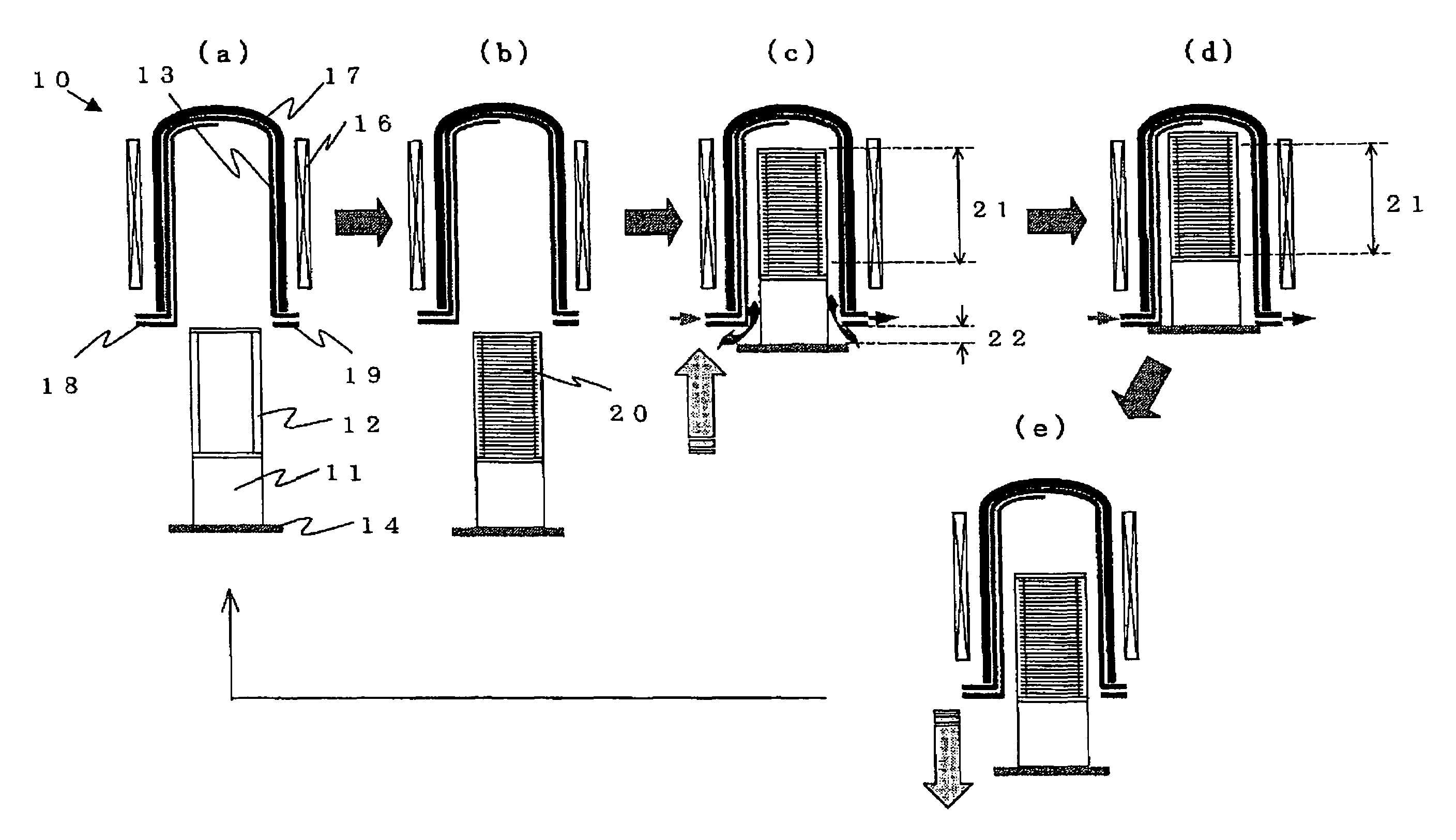
[0063]Silicon wafers having a diameter of 200 mm were heat-treated according to the procedure as shown in FIG. 1. The silicon wafer used in the heat treatment was a P type (doped with boron) and had a resistivity of 8-12 Ωcm, a plane orientation of (100), and a nitrogen concentration of 8×10¹³ atoms / cm3.

[0064]First, fifty silicon wafers 20 were placed in the boat 12 supported by the support member 11 (FIG. 1(a)(b)). In this case, five wafers from the upper side of the boat 12 and ten wafers from the lower side were set to serve as dummy wafers that were not to be products, and the semiconductor wafers to be products were placed between the dummy wafers placed in the upper side and in the lower side of the boat 12. The length of the part for placing wafers in the boat 12 was 945 mm.

[0065]Next, the boat 12 in which the silicon wafers 20 were placed was inserted in the furnace tube 13 (FIG. 1(c)). That is, into the furnace in which the temperature of the thermally uniform portion 21 wa...

example 2

[0070]Annealed wafers were produced in the same method as Example 1 except that when the boat 12 in which the silicon wafers 20 were placed was inserted into the furnace tube 13 (FIG. 1(c)), after the interval 22 between the furnace tube 13 and the shutter 14 became 25 mm by inserting the boat 12 at a constant rate of 100 mm / min, the boat 12 was inserted at an insertion rate of 25 mm / min and the furnace tube 13 was blocked in with the shutter 14. In addition, the state that the entirety of the silicon wafers to be products was in the thermally uniform portion 21 and that the interval 22 between the furnace tube 13 and the shutter 14 existed was maintained for 1 min.

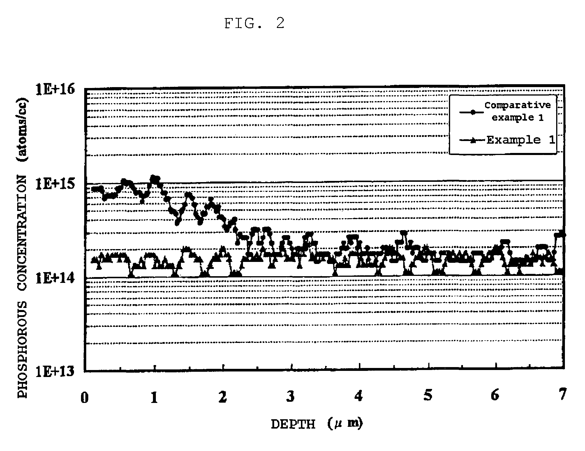
[0071]Similarly to Example 1, in the both wafers in the bottom and the top, resistivity was 8-12 Ωcm. Thereby, it was found that the resistivity hardly changed before and after the heat treatment, and that there was extremely little contamination with phosphorous during the heat treatment (both resistivity and SIMS profil...


PUM


Abstract

The present invention is a method for producing an annealed wafer, wherein, at least, when a boat in which a semiconductor wafer is placed is inserted into a furnace tube, the boat is inserted along with introducing an inert gas into the furnace, so that entirety of the semiconductor wafer to be a product reaches a thermally uniform portion, then an insertion rate of the boat in which the semiconductor wafer is placed is decelerated and / or suspended, so that an interval between the furnace tube and the shutter is maintained for a predetermined time, and then the furnace tube is blocked in with the shutter. Thereby, there can be provided a method for producing an annealed wafer by which during the heat treatment, it can be more certainly prevented that the wafer is contaminated with conductive impurities and that thereby resistivity of the wafer is changed before and after the heat treatment.

Description

TECHNICAL FIELD[0001]The present invention relates to a method for producing an annealed wafer in which Grown-in defects and so forth that are COP (Crystal Originated Particle) in a surface of a semiconductor wafer and a source of the COP and so forth, which exist from surface to a depth of some micrometers in a surface layer of the semiconductor wafer, are effectively made to disappear, and more particularly, relates to a method comprising, performing a high-temperature heat treatment under an atmosphere of an inert gas such as argon or an reducing gas such as hydrogen so that COP defects and so forth in the vicinity of the surface are made to disappear, preventing contamination with conductive impurities, and thereby producing an annealed wafer of high quality.BACKGROUND ART[0002]A semiconductor wafer used in the present-day production of a semiconductor device is made of silicon produced by, for example, Czochralski method (CZ method). In the device process, the temperature has b...

Claims


Application Information

Patent Timeline
Patent Type & Authority Patents(United States)
IPC IPC(8): H01L21/00
CPCH01L21/67757H01L21/324H01L21/2251
Inventor NAGOYA, TAKATOSHI
Owner SHIN-ETSU HANDOTAI CO LTD
Why Eureka
Try Eureka