Substrate with pin, manufacturing method thereof, and semiconductor product

a manufacturing method and semiconductor technology, applied in the direction of printed circuit aspects, sustainable manufacturing/processing, final product manufacturing, etc., can solve the problems of insufficient strength inability to dispose of the core substrate for reinforcement, and 1 mm or less of the wiring substrate, so as to achieve manufacturing surely and easily, and the effect of easy manufactur

a manufacturing method and semiconductor technology, applied in the direction of printed circuit aspects, sustainable manufacturing/processing, final product manufacturing, etc., can solve the problems of insufficient strength inability to dispose of the core substrate for reinforcement, and 1 mm or less of the wiring substrate, so as to achieve manufacturing surely and easily, and the effect of easy manufactur

US20080296752A1Active Publication Date: 2008-12-04SHINKO ELECTRIC IND CO LTD

Image

  • Substrate with pin, manufacturing method thereof, and semiconductor product
  • Substrate with pin, manufacturing method thereof, and semiconductor product
  • Substrate with pin, manufacturing method thereof, and semiconductor product

Examples


Embodiment Construction

[0046]A preferred embodiment of the invention will hereinafter be described in detail with reference to the accompanying drawings.

(Substrate with Pin)

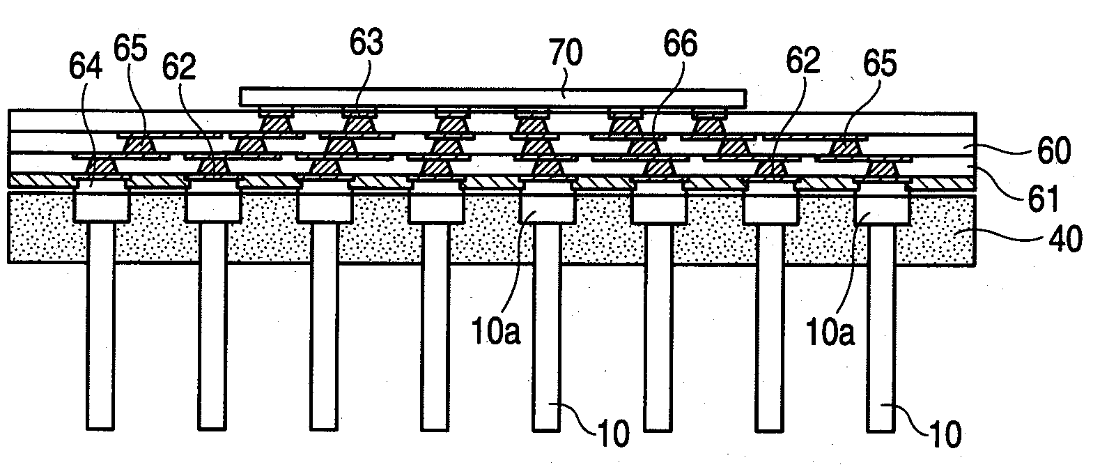
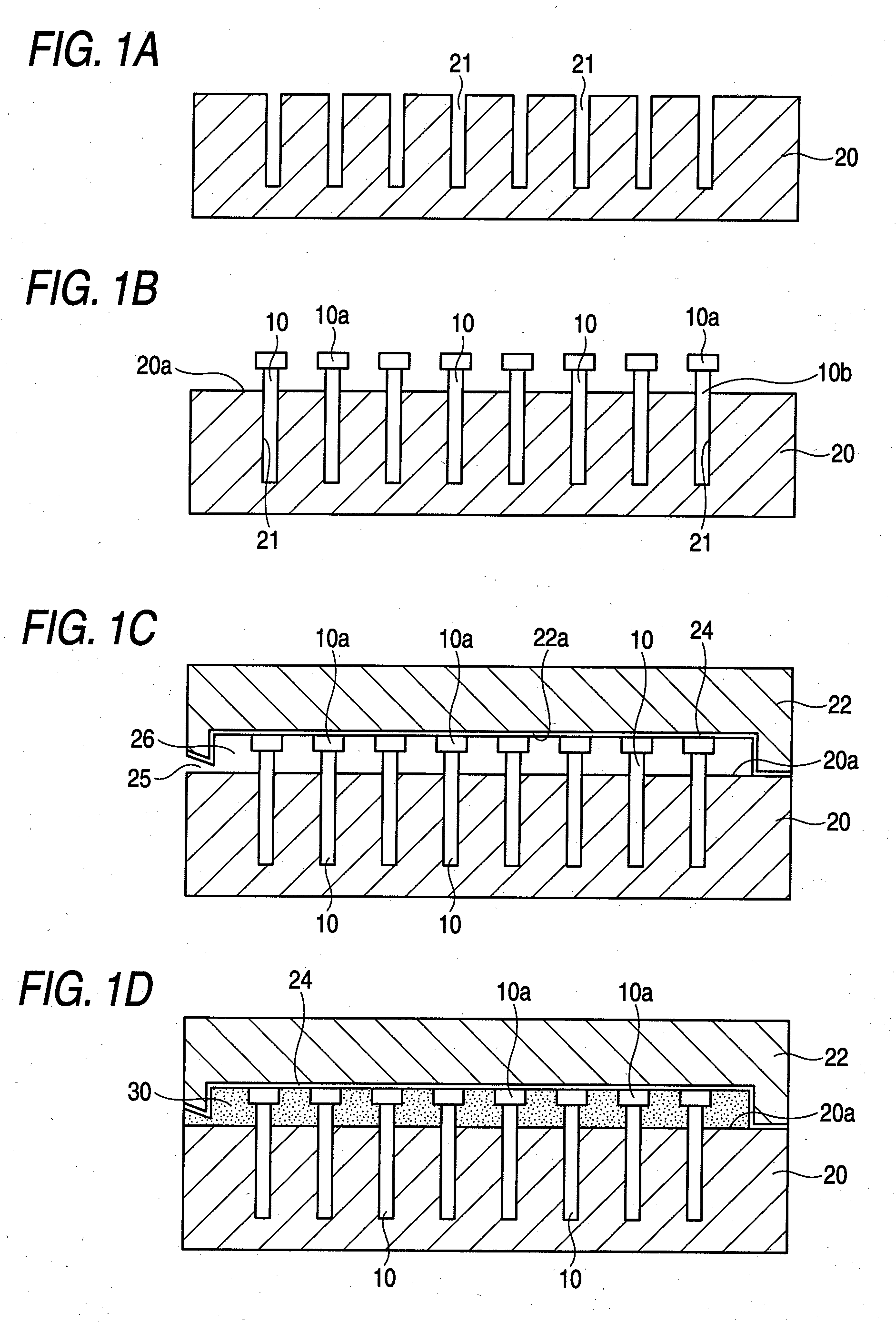
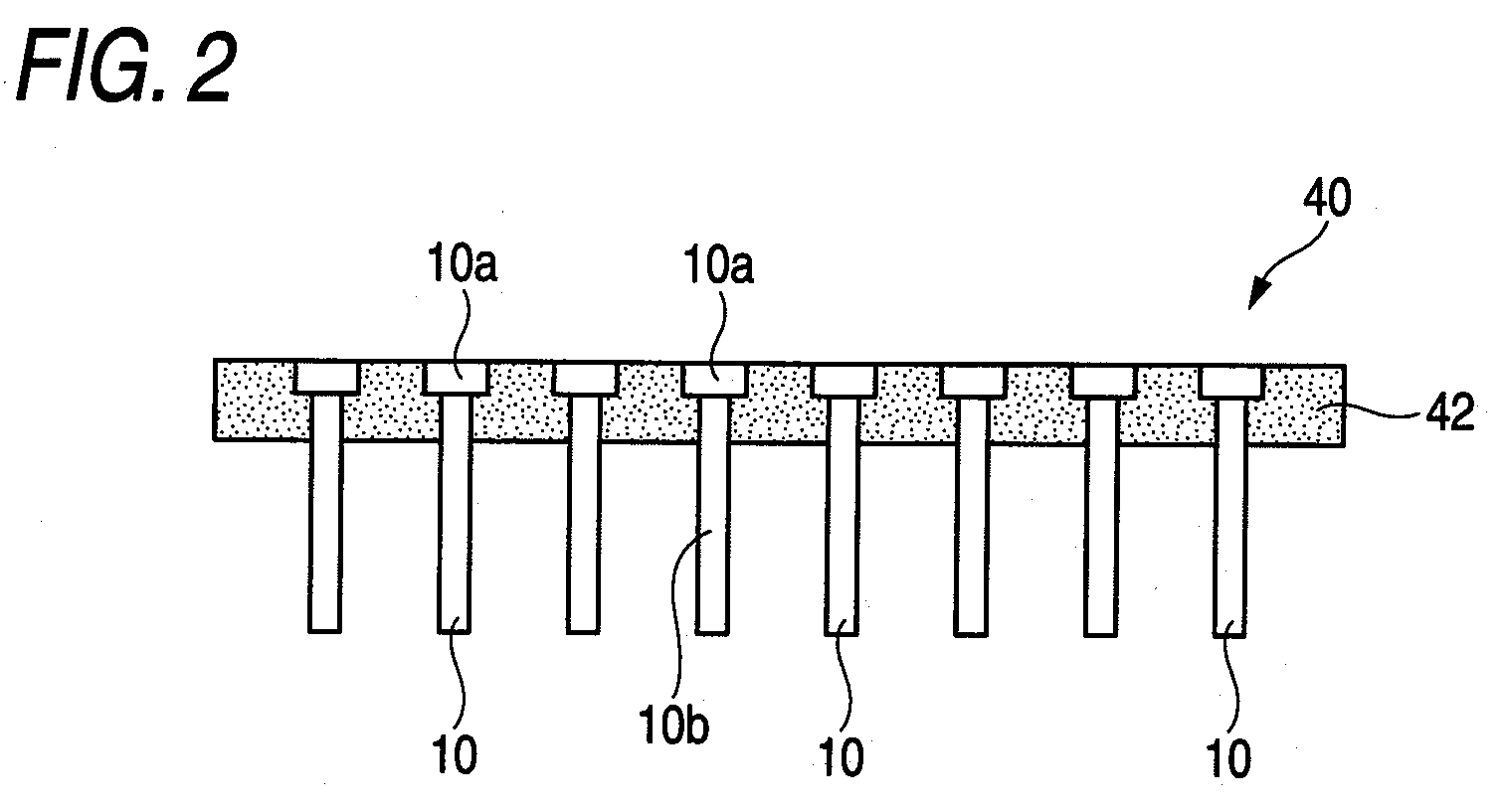
[0047]FIGS. 1A to 1D show a manufacturing method of a substrate with pins according to the invention. The substrate with the pins according to the invention is formed in a form erected by aligning pins 10 with a substrate molded in a flat plate shape by a molding resin in predetermined arrangement.

[0048]FIG. 1A shows a lower mold 20 of a metal mold for molding in which the pins 10 are supported in a predetermined array. Multiple set holes 21 for supporting the pins 10 in alignment with a plane array of the pins 10 in the substrate with the pins are formed in the lower mold 20. The set hole 21 is formed in an inside diameter in which a shaft part of the pin 10 is slid. In the pin 10 attached to the substrate with the pins, an outside diameter of a head part 10a is about 0.75 mm and an outside diameter of the shaft part is about 0.3 mm.

[...


PUM

PropertyMeasurementUnit
thicknessaaaaaaaaaa
diameteraaaaaaaaaa
diameteraaaaaaaaaa

Abstract

A semiconductor product is constructed of a wiring substrate in which pads for pin connection are formed, and a substrate with pins in which pins are disposed. The substrate with the pins is formed so that one end of the pin is exposed to one surface of a resin substrate formed by resin molding and the other end of the pin extends from the other surface of the resin substrate and one end of the pin is bonded to a pad of the wiring substrate through a conductive material.

Description

[0001]This application claims priority to Japanese Patent Application No. 2007-119040, filed Apr. 27, 2007, in the Japanese Patent Office. The Japanese Patent Application No. 2007-119040 is incorporated by reference in its entirety.TECHNICAL FIELD[0002]The present disclosure relates to a substrate with a pin used in a PGA (Pin Grid Array) type semiconductor device, a preferred manufacturing method of the substrate with the pin, and a semiconductor product using the substrate with the pin.RELATED ART[0003]A PGA type semiconductor device has an advantage that the semiconductor device can be mounted by only inserting a pin into a socket and the need for a complicated step of mounting by solder reflow as described in a BGA type semiconductor device is eliminated, and an advantage that a product can be replaced by only reinserting the product from the socket, and is used in various electronic products.[0004]The PGA type semiconductor device includes a product manufactured by disposing a ...

Claims


Application Information

Patent Timeline
04 Dec 2008
Publication
US20080296752A1
IPC
H01L23/49; H05K1/00; H05K3/00
CPC
H01L21/4853; H01L23/49833; H01L23/49861; H05K3/303; Y10T29/49147; H05K2201/10318; H05K2201/10424; H01L2224/16225
Inventors
NAKAJIMA, SHIGEO