Device for measuring metal/semiconductor contact resistivity

Inactive Publication Date: 2008-12-04
COMMISSARIAT A LENERGIE ATOMIQUE ET AUX ENERGIES ALTERNATIVES
View PDF12 Cites 15 Cited by
  • Summary
  • Abstract
  • Description
  • Claims
  • Application Information

AI Technical Summary

Benefits of technology

[0042]The linear regression of the function R=f(L) and/or the calculation of ρc may be performed for all o

Problems solved by technology

However, this CKR device is only suitable for measuring the contact resistivity of a horizontal interface between the first metal 6 and the semiconductor 2, i.e., parallel to the plane formed by the semiconductor substrate 2.
Thus, with this device, it is difficult to extract an exact value of the specific contact resistivity of the interface.
However, in these two cases, as described in the document “2D simulations for accurate extraction of the specific contact resistivity from contact resistance data” by W. M.

Method used


Image

  • Device for measuring metal/semiconductor contact resistivity
  • Device for measuring metal/semiconductor contact resistivity
  • Device for measuring metal/semiconductor contact resistivity

Examples


Embodiment Construction

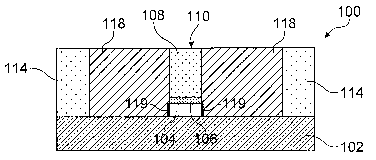
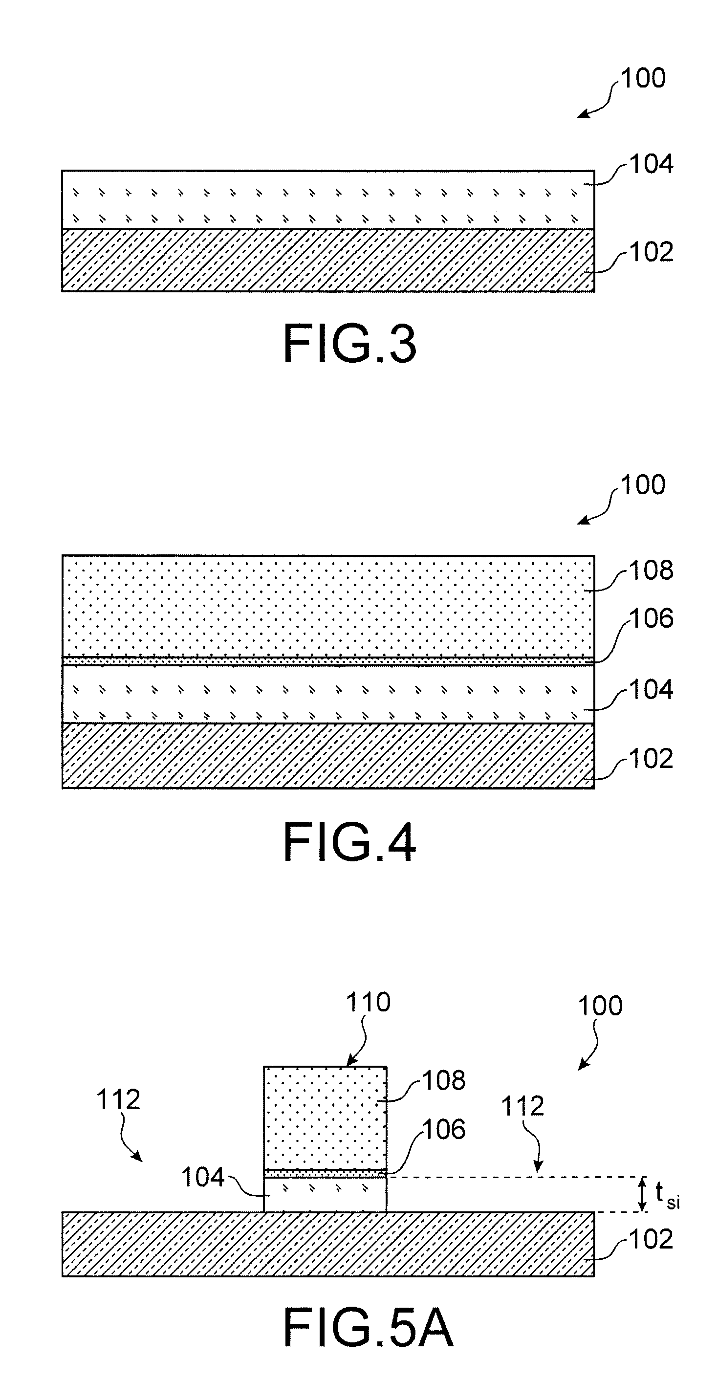
[0086]Reference is made first to FIGS. 3 to 8, which show the steps of a process for manufacturing a device 100 for measuring the resistivity of an interface between a semiconductor and a metal.

[0087]As shown in FIG. 3, the process is implemented by starting with a stack comprising a dielectric layer 102, in this case being oxide-based and having a thickness equal to approximately 145 nm, on which is deposited a semiconductor-based layer 104 intended to form the interface, e.g., made of silicon, and having a thickness equal to approximately 70 nm. In this case, the dielectric layer 102 and the semiconductor-based layer 104 thus form an SOI-type substrate. In one alternative, the semiconductor of layer 104 could likewise be germanium, then forming, together with the dielectric layer 102, a GeOI (germanium-on-insulator) type substrate. The dielectric layer 102 and the semiconductor-based layer 104 generally form a semiconductor-on-insulator type substrate.

[0088]The thickness tsi of th...


PUM

PropertyMeasurementUnit
Thicknessaaaaaaaaaa
Thicknessaaaaaaaaaa
Thicknessaaaaaaaaaa

Abstract

A device for measuring the resistivity ρc of an interface between a semiconductor and a metal, comprising at least:
    • one dielectric layer,
    • at least one semiconductor-based element of a substantially rectangular shape, which is arranged on the dielectric layer, having a lengthwise L and widthwise W face in contact with the dielectric layer and having a thickness t,
    • at least two interface portions containing the metal or an alloy of said semiconductor and said metal,
each of the two opposing faces of the semiconductor element, having a surface equal to t×W and being perpendicular to the face in contact with the dielectric layer, being completely covered by one of the interface portions.

Description

TECHNICAL FIELD AND PRIOR ART[0001]This document relates to a device enabling accurate measurement of the contact resistivity of an interface between a semiconductor and a metal, or an alloy (of the metal and the semiconductor) and the semiconductor. This device is more particularly suitable to vertical interfaces the dimensions of which correspond to those that are found in current thin-film transistors, e.g., formed by the lateral surface of an element having a thickness of between approximately 1 nm and 50 nm and a width of between approximately 30 nm and a few micrometers (typically 2 μm).[0002]The device can be used for accurately characterizing electrical parameters of materials, or for optimizing metal source and drain CMOS transistors by the choice of materials.[0003]Several types of devices currently exist for measuring the contact resistivity between a metal and a semiconductor.[0004]Devices of the “Cross Kelvin Resistor” type (CKR) enable measurement of the Kelvin resista...

Claims


Application Information

Patent Timeline
IPC IPC(8): G01R31/26G01R31/28
CPCH01L22/34H01L2924/0002Y10T29/49004H01L2924/00
Inventor VINET, MAUD
Owner COMMISSARIAT A LENERGIE ATOMIQUE ET AUX ENERGIES ALTERNATIVES
Why Eureka
Try Eureka