

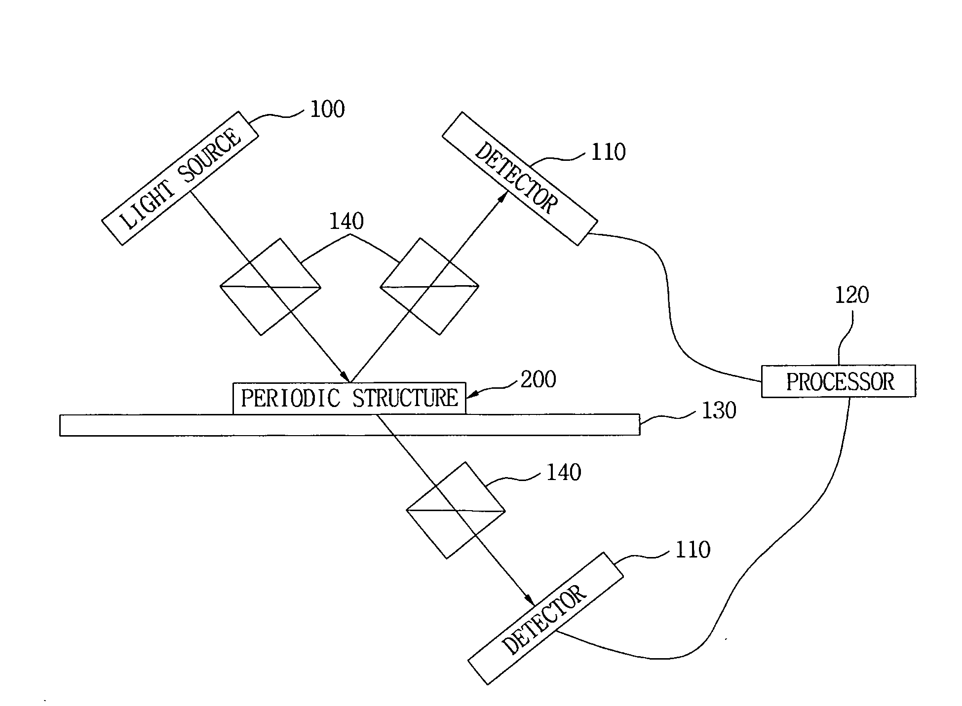
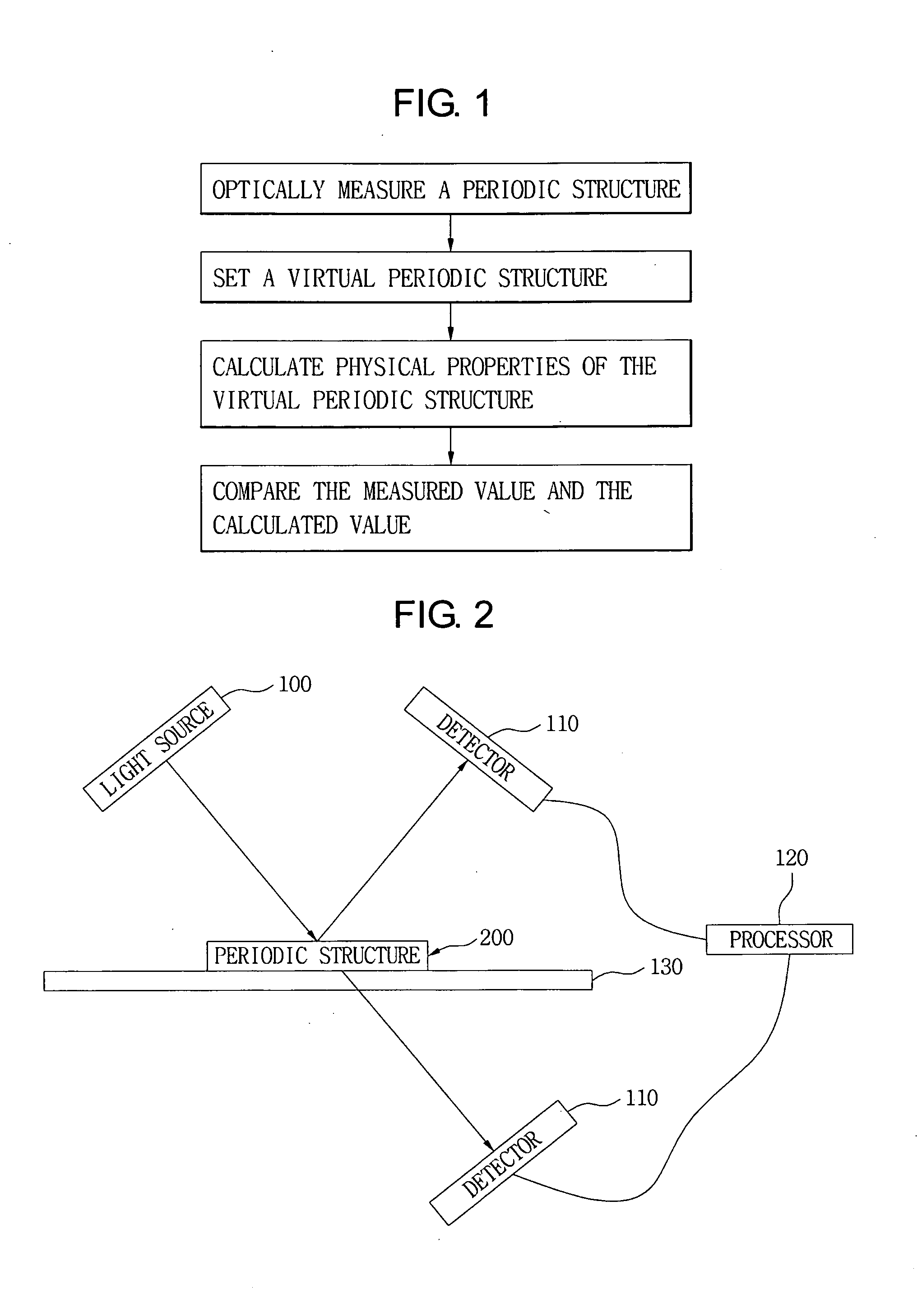
Method for determining physical properties of a multilayered periodic structure
a multi-layered, periodic structure technology, applied in the direction of instruments, measurement devices, scientific instruments, etc., can solve the problems of insufficient resolution of the pattern tester, inability to perform an accurate analysis, and difficulty in determining the physical properties of the multi-layered periodic structur
- Summary
- Abstract
- Description
- Claims
- Application Information
AI Technical Summary
Benefits of technology
Problems solved by technology
Method used
Image

Examples
embodiment
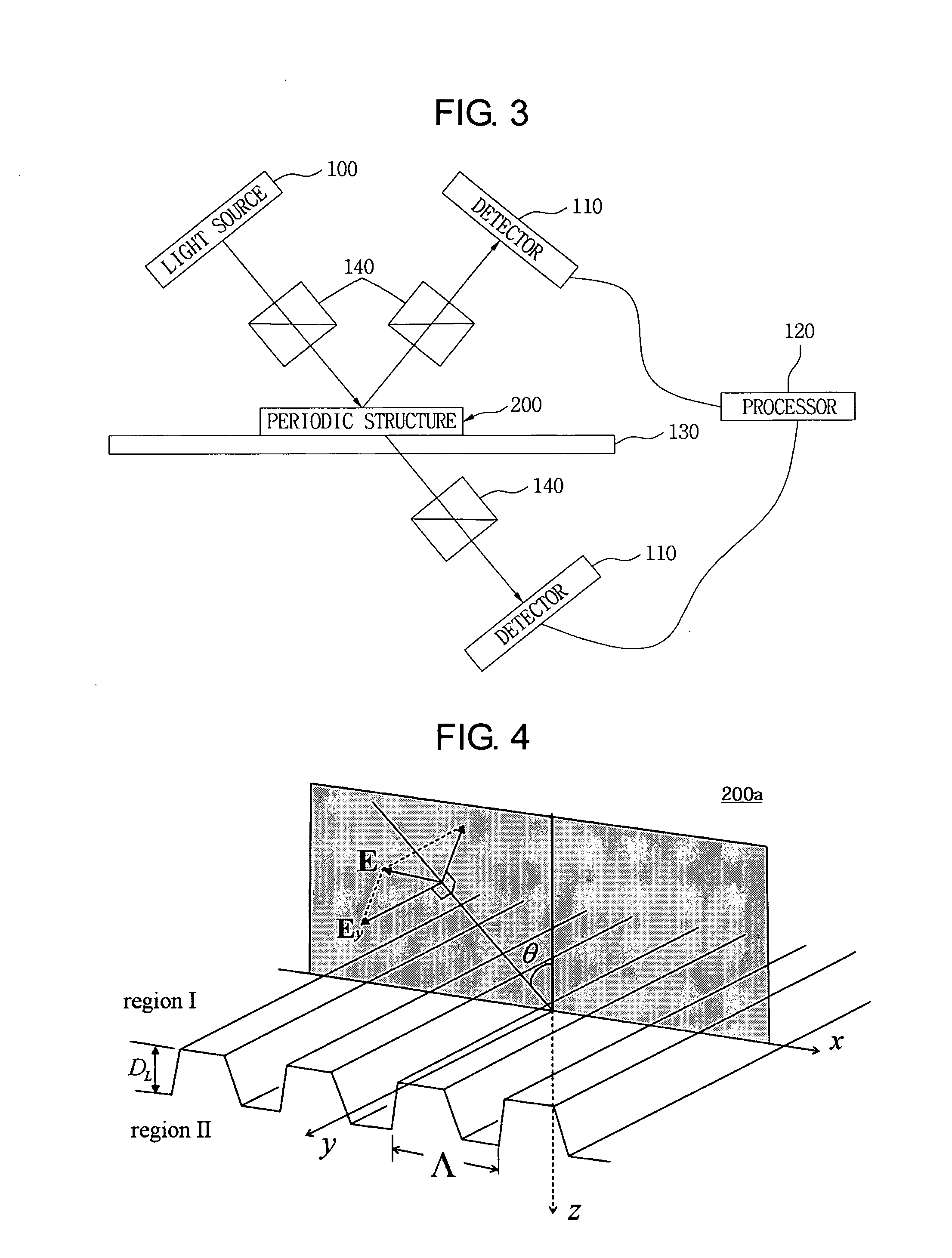
[0056]As an embodiment of the present invention, a virtual periodic structure where a surface layer is formed is set as illustrated in FIG. 8. This virtual periodic structure has a repeated period of 60 nm. The thickness of a ridge region formed of silicon crystals is 45 nm, an oxide is formed on the surface of the ridge region to the thickness of 5 nm, and the slope of a ridge is set as 81°.
[0057]The slope and period of the virtual periodic structure and the width and height of the ridge may be varied as random values. Further, the geometrical shape thereof may have a random shape.
[0058]The physical properties of the virtual periodic structure are calculated by using the method according to an embodiment of the present invention, to be compared with the measured values of a real periodic structure.
[0059]FIGS. 9 and 10 are graphs respectively illustrating results of the calculated reflectivity of the virtual periodic structure considering the oxide layer as illustrated in FIG. 8 and...
PUM
| Property | Measurement | Unit |
|---|---|---|
| thickness | aaaaa | aaaaa |
| thickness | aaaaa | aaaaa |
| physical properties | aaaaa | aaaaa |
Abstract
Description
Claims
Application Information