Method for fabricating photodiode

a technology of photodiodes and photodiodes, which is applied in the direction of photovoltaic energy generation, electrical equipment, semiconductor devices, etc., can solve the problems of noise generated by dark current, ccd consumes a large amount of power, and the size of ccd is not easy to reduce, so as to reduce the noise of dark current, prevent the lattice structure from being damaged, and increase the sensitivity of the photodiode

Inactive Publication Date: 2008-12-04
UNITED MICROELECTRONICS CORP
View PDF5 Cites 4 Cited by
  • Summary
  • Abstract
  • Description
  • Claims
  • Application Information

AI Technical Summary

Benefits of technology

[0024]The method for fabricating the photodiode in the present invention can prevent the lattice structure from being damaged during the high-energy implantation process. Therefore, the dark current can be reduced and the sensitivity of the photodiode will be increased. Moreover, the distance for the light current to the gate channel is reduced, therefore the signal can be sent more quickly. Furthermore, the surface of the photo sensor area of the photodiode in the present invention is increased, thus the sensitivity of the photodiode is increased as well. The depletion region of the photodiode in the present invention is near the surface of photo sensor area, thus the photodiode in the present invention has a better sensitivity to short wavelength light. In addition, because the depletion region of the photodiode in the present invention is far from the STI structure, the leakage between the photodiode and the STI structure can be reduced.

Problems solved by technology

Because the fabricating process of a CCD is complicated, and the process is difficult to be integrated into the control circuit or the signal processing system, the size of the CCD is not easy to reduced.
Furthermore the CCD consumes a high amount of power.
For example, light current serves as signal data which is generated when the photo sensor area is illuminated, and dark current is noise which is generated when the photo sensor area is without light.
However, the fabricating process of the multi-trench photodiode is very complicated.
The lattice structure will be damaged easily during the high-energy implantation process.

Method used


Image

  • Method for fabricating photodiode
  • Method for fabricating photodiode
  • Method for fabricating photodiode

Examples


first embodiment

[0031]Please refer to FIG. 15 to FIG. 19. FIG. 15 to 19 are schematic diagrams illustrating the method for fabricating a photodiode in accordance with the present invention.

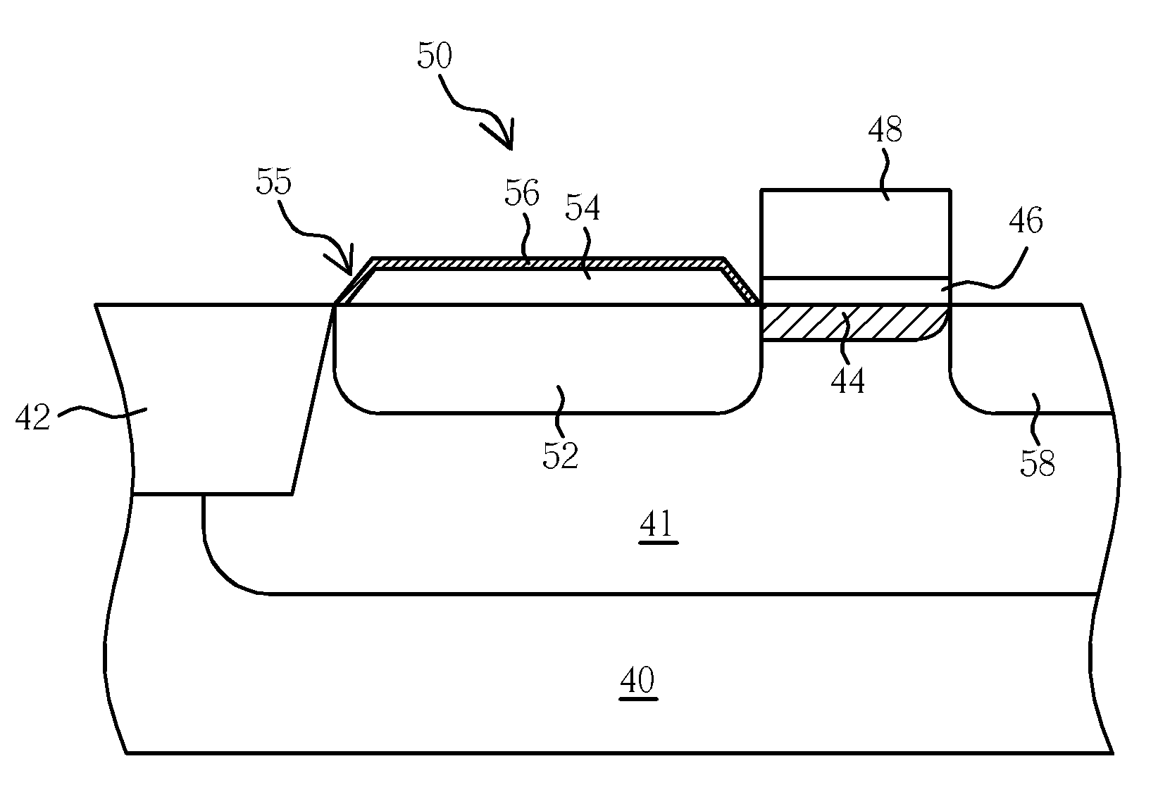
[0032]As shown in FIG. 15, first providing a substrate 40 comprises a P-type well 41 and a STI structure 42. These processes are well-known for those skilled in the art, for example, performing a well forming process, next, forming at least a trench (not shown) in the substrate 40 and forming an insulator (not shown) to cover the substrate 40 and filling up the trench. Following that, a STI structure 42 is formed in the substrate 40. The STI structure 42 isolates the unit pixels of the CMOS image sensor one from another. The STI structure can be replaced by other insulated structures such as field oxide. After that, a third doping region, the P-type doping region 44, is formed in the substrate 40 by the implantation process to adjust the threshold voltage of the transfer gate.

[0033]Referring to FIG. 16, a dielect...

second embodiment

[0039]Please refer to FIG. 20 to FIG. 24. FIG. 20 to 24 are schematic diagrams illustrating the method for fabricating a photodiode in accordance with the present invention.

[0040]As shown in FIG. 20, a substrate 40 comprising a P-type well 41 and a STI structure 42 is provided first. These processes are well-known for those skilled in the art, for example, performing a well forming process, next, forming at least a trench (not shown) in the substrate 40 and forming an insulator (not shown) to cover the substrate 40 and filling up the trench. Following that, a STI structure 42 is formed in the substrate 40. The STI structure isolates the unit pixels of the CMOS image sensor one from another. The STI structure can be replaced by other insulated structure such as field oxide. After that, a third doing region, the P-type doping region 44, is formed in the substrate 40 by the implantation process to adjust the threshold voltage of the transfer gate.

[0041]Referring to FIG. 21, a dielectri...


PUM

PropertyMeasurementUnit
conductiveaaaaaaaaaa
insulatoraaaaaaaaaa
lattice structureaaaaaaaaaa

Abstract

A method of fabricating photodiode includes: a substrate comprising a well is provided, next, a first doping region is formed in the well, following that a conductive layer is formed on the surface of the first doping region by an epitaxial growth process, meanwhile, the conductive layer is in-situ doped to form a second doping region in the conductive layer. The method for fabricating the photodiode in the present invention can prevent the lattice structure from being damaged during the high dozes implantation process. Therefore, the dark current can be reduced and the sensitivity of the photodiode will be increased.

Description

BACKGROUND OF THE INVENTION[0001]1. Field of the Invention[0002]The present invention relates generally to methods of fabricating a photodiode and more particularly, to methods which can prevent the lattice structure of the photodiode from being damaged during the high-energy implantation process.[0003]2. Description of the Prior Art[0004]A complementary metal-oxide-semiconductor (CMOS) image sensor is a common solid-state image sensor. The CMOS image sensors have been gradually replacing charge-coupled devices (CCD) over time. Because the fabricating process of a CCD is complicated, and the process is difficult to be integrated into the control circuit or the signal processing system, the size of the CCD is not easy to reduced. Furthermore the CCD consumes a high amount of power. On the contrary, the CMOS image sensors are manufactured by traditional semiconductor manufacturers, and have lower costs and smaller sizes than regular image sensors. Furthermore, CMOS image sensors have ...

Claims


Application Information

Patent Timeline
Patent Type & Authority Applications(United States)
IPC IPC(8): H01L21/00
CPCH01L27/14603H01L27/14689H01L31/103H01L31/1804Y02E10/547
Inventor LAN, BANG-CHIANGSU, TZUNG-IKUO, CHIEN-NANSU, CHAO-ANLIN, HENG-CHINGLI, SHIH-WEIHUNG, WEI-CHIN
Owner UNITED MICROELECTRONICS CORP
Why Eureka
Try Eureka