Electronic component and manufacturing method thereof

Inactive Publication Date: 2008-12-18
NIHON DEMPA KOGYO CO LTD
View PDF4 Cites 16 Cited by
  • Summary
  • Abstract
  • Description
  • Claims
  • Application Information

AI Technical Summary

Benefits of technology

[0021]It is possible to prevent defects arising when resin-sealing electronic components, caused by leakage defects, resin interfusion defects, or the like, and it is possible to easily resin-seal a number of electronic components all together.

Problems solved by technology

The problem to be solved by the present invention is that when manufacturing, by resin-sealing, electronic components having no defects such as leakage defects, resin interfusion defects or the like, it is not possible to process a number of chip-mounted collective substrates all together, and a new and expensive manufacturing facility is required.

Method used


Image

  • Electronic component and manufacturing method thereof
  • Electronic component and manufacturing method thereof
  • Electronic component and manufacturing method thereof

Examples


Embodiment Construction

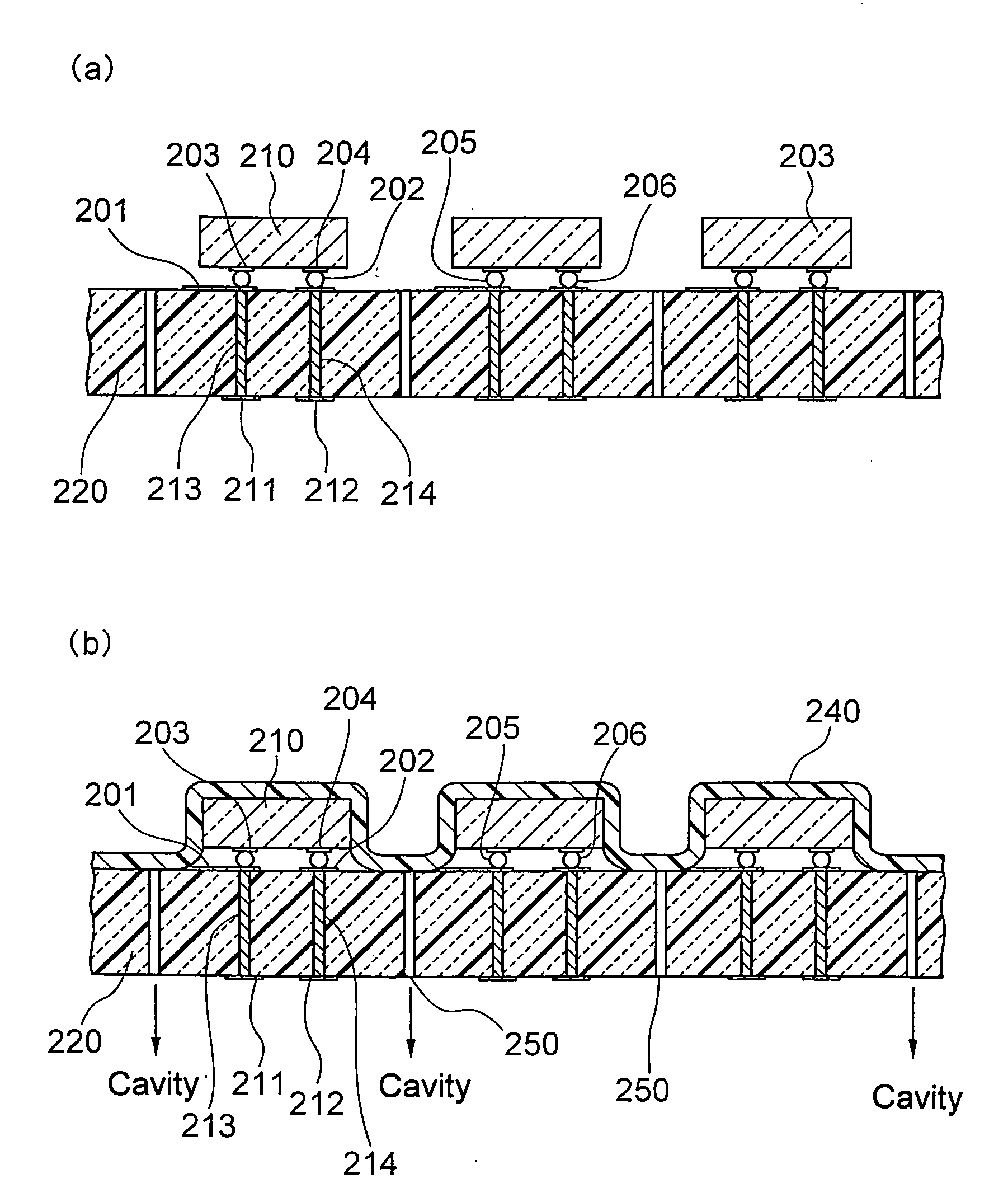
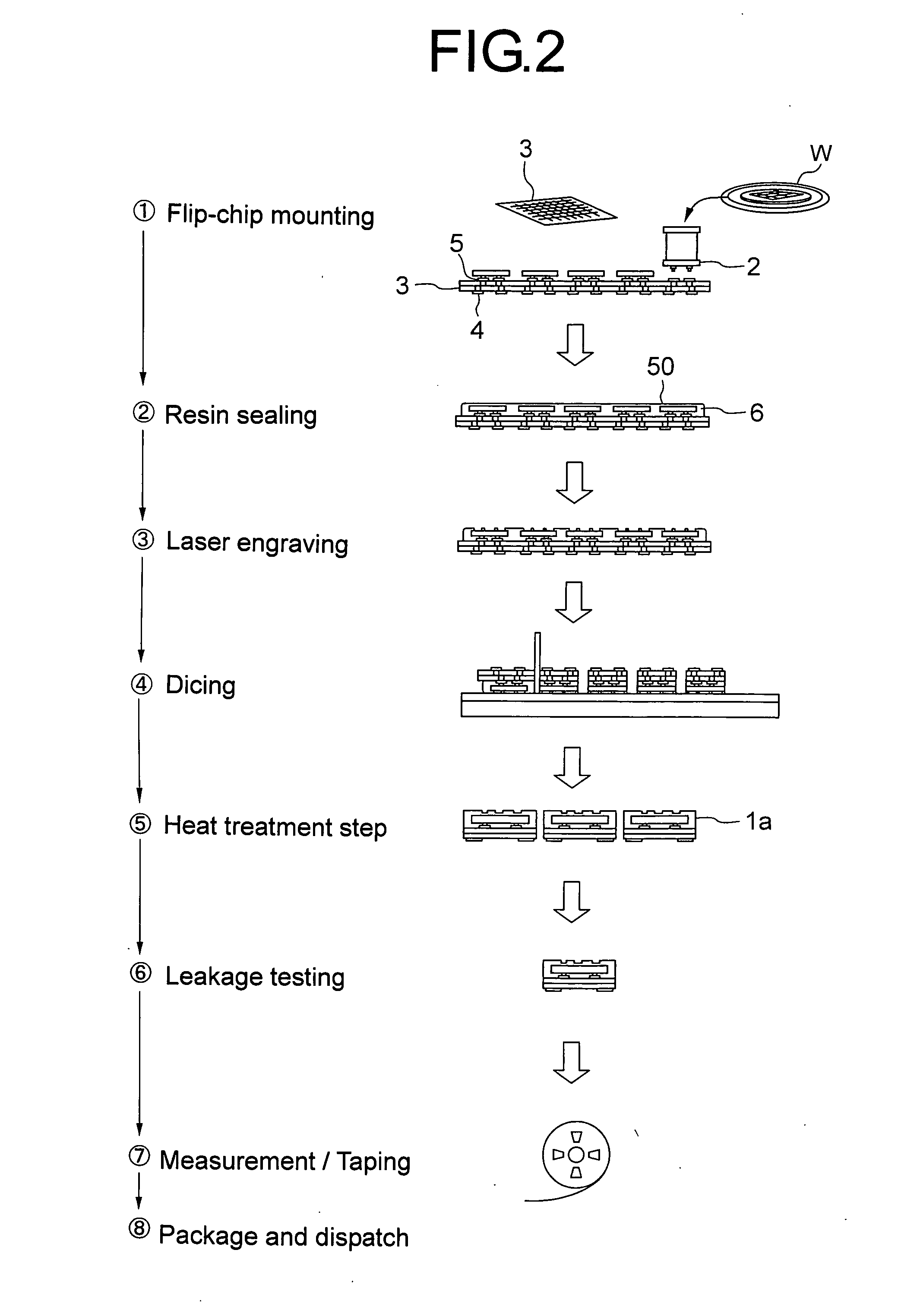
[0029]Hereinafter, a manufacturing method of an electronic component of the present invention is described in detail for a manufacturing method of an embodiment of a mount type surface acoustic wave device (hereinafter, referred to as “SAW device”).

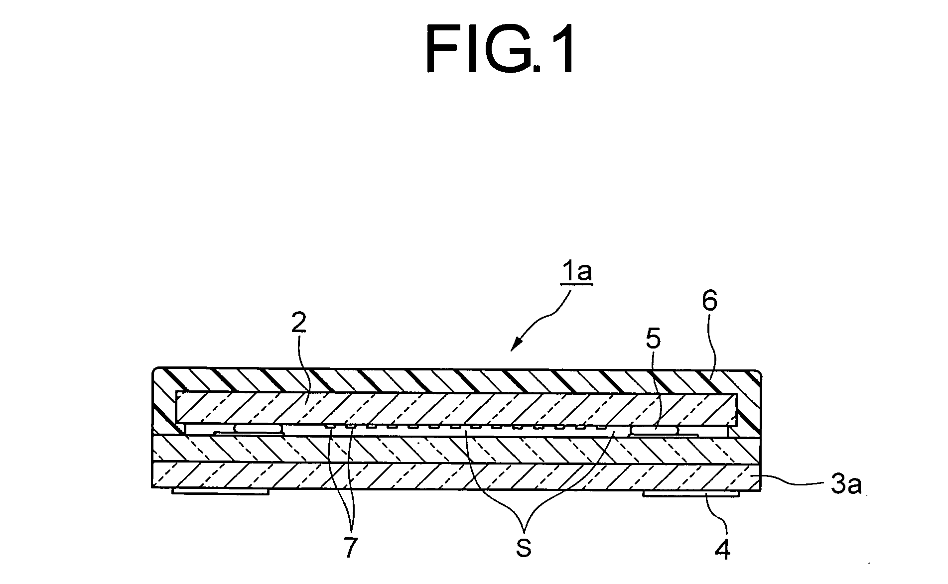
[0030]FIG. 1 shows a vertical sectional view of a SAW device la to be manufactured in a SAW device manufacturing method that is an embodiment of an electronic component manufacturing method of the present invention.

[0031]This SAW device 1a (piezoelectric component) comprises: a ceramic substrate (insulating substrate) 3a formed by laminating a plurality of ceramic; a SAW chip 2 that is formed from lithium tantalite (LiTaO3) or the like for example and that is mounted on the top face of this ceramic substrate 3a via gold bumps 5; an epoxy resin (resin sealing section) 6 that resin-seals this SAW chip 2; and external electrodes 4 mounted on the bottom face of the ceramic substrate 3. The SAW chip 2 is sealed by for example an epoxy resin so...


PUM

PropertyMeasurementUnit
Pressureaaaaaaaaaa
Wavelengthaaaaaaaaaa

Abstract

It is possible to prevent defects arising when resin-sealing electronic components, caused by leakage defects, resin interfusion defects, or the like, and it is possible to easily resin-seal a number of electronic components all together. There is provided a method of manufacturing electronic components on which SAW chips are mounted by face down bonding on wiring electrodes formed on a main face of a collective substrate, comprising the steps of: placing a resin sheet on the main face of the collective substrate, on which the SAW chips have been mounted; accommodating the collective substrate, on which the SAW chips have been mounted, in a flexible and sealed bag, and then seal-closing the sealed bag; submerging the accommodating bag into a pressurized container filled with a liquid, and then sealing off the pressurized container; supplying a pressurizing fluid into the pressurized container, raising the pressure within the pressurized container, carrying out heat application to heat-cure the resin sheet, and thereby tightly adhering the resin sheet onto the main face side of the SAW chips and the collective substrate, on which the SAW chips have been mounted so as to resin-seal the collective substrate; taking out the sealed bag from the pressurized container; taking out the resin-sealed collective substrate, on which the SAW chips have been mounted, from the sealed bag; and cutting the resin-sealed collective substrate, which has been taken out, into individual pieces.

Description

BACKGROUND OF THE INVENTION[0001]The present invention relates to a piezoelectric component and a manufacturing method thereof, such that in a method of manufacturing a SAW device in which a SAW chip is sealed by a resin after an electronic component such as a surface acoustic wave (SAW) chip has been mounted on a mounting substrate by face down bonding using bumps, it is possible to manufacture using a simple method, a large number of piezoelectric devices all together, while preventing defects in products caused by leakage defects, resin infiltration defects, or the like.[0002]A surface acoustic wave device (SAW device) is mounted in a mobile phone and is configured with patterns of comb shaped electrodes (IDT electrodes), and connection pads or the like arranged on a piezoelectric substrate such as crystal piezoelectric substrate and lithium tantalite substrate, wherein surface acoustic waves are excited by applying a high frequency electric field to the IDT electrodes, and a fil...

Claims


Application Information

Patent Timeline
IPC IPC(8): B32B37/00
CPCB29C43/06B29C43/12H01L2924/1461H01L2224/16225H01L2924/01074B29C43/18B29C43/222B29C43/3697B29C43/46B29C2043/3238B29C2043/3649B29K2105/256H01L21/56H01L23/315H01L24/97H01L2224/97H01L2924/01013H01L2924/01057H01L2924/01079H01L2924/01082H01L2924/01005H01L2924/01006H01L2924/01023H01L2924/01033H01L2224/81H01L2924/00H01L2224/0554H01L2224/05568H01L2224/05573H01L2924/00014H01L2924/15787H01L2924/181H01L2224/05599H01L2224/0555H01L2224/0556
Inventor SAKAIRI, NATSUHIKOKOSHIKAWA, TOMOMIODA, SEIJITSUDA, TOSHIMASA
Owner NIHON DEMPA KOGYO CO LTD
Why Eureka
Try Eureka