

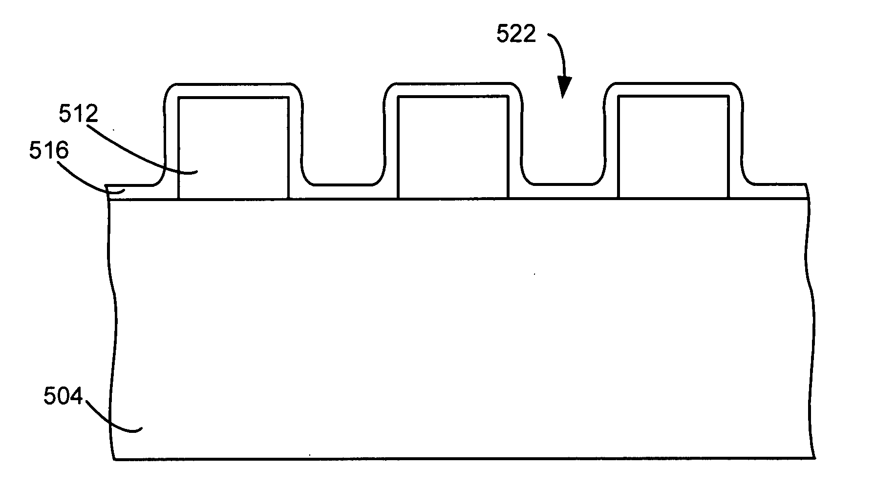
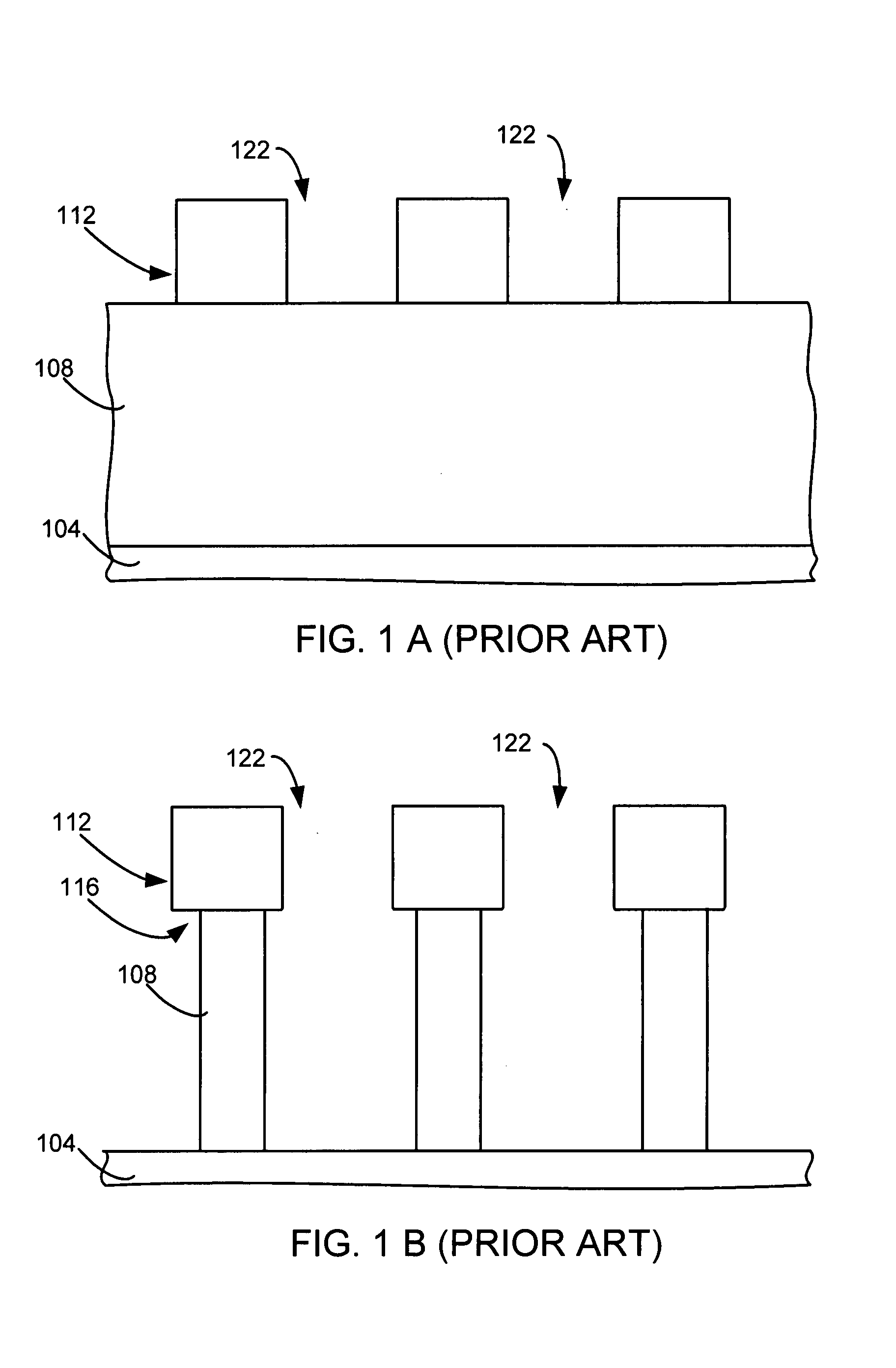
Minimization of mask undercut on deep silicon etch
a technology of deep silicon and undercutting, which is applied in the direction of electrical equipment, decorative surface effects, decorative arts, etc., can solve the problem of more severe undercutting
- Summary
- Abstract
- Description
- Claims
- Application Information
AI Technical Summary
Benefits of technology
Problems solved by technology
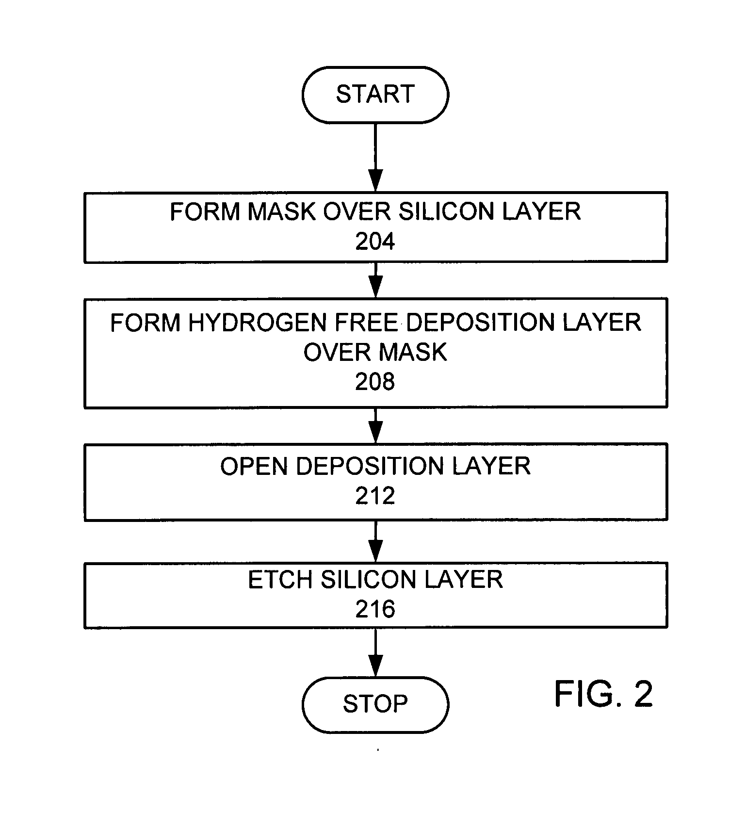
Method used
Image

Examples
example
[0020]In an example of an implementation of the invention, FIG. 3 illustrates a processing tool that may be used in an implementation of the invention. FIG. 3 is a schematic view of a plasma processing system 300, including a plasma processing tool 301. The plasma processing tool 301 is an inductively coupled plasma etching tool and includes a plasma reactor 302 having a plasma processing chamber 304 therein. A transformer coupled power (TCP) controller 350 and a bias power controller 355, respectively, control a TCP power supply 351 and a bias power supply 356 influencing the plasma 324 created within plasma chamber 304.
[0021]The TCP power controller 350 sets a set point for TCP power supply 351 configured to supply a radio frequency signal at 13.56 MHz, tuned by a TCP match network 352, to a TCP coil 353 located near the plasma chamber 304. An RF transparent window 354 is provided to separate TCP coil 353 from plasma chamber 304 while allowing energy to pass from TCP coil 353 to p...
PUM
| Property | Measurement | Unit |
|---|---|---|
| thick | aaaaa | aaaaa |
| radio frequency | aaaaa | aaaaa |
| thick | aaaaa | aaaaa |
Abstract
Description
Claims
Application Information