Alternating Self-Assembling Morphologies of Diblock Copolymers Controlled by Variations in Surfaces

a technology of diblock copolymer and surface variation, which is applied in the direction of resistor manufacturing, liquid/solution decomposition chemical coating, photomechanical treatment, etc., can solve the problems of inability to accommodate the fabrication of structures and features at the nanometer level, and require a more complex layout of elements

Active Publication Date: 2008-12-18
MICRON TECH INC
View PDF99 Cites 105 Cited by
  • Summary
  • Abstract
  • Description
  • Claims
  • Application Information

AI Technical Summary

Problems solved by technology

Optical lithographic processing methods are not able to accommodate fabrication of structures and features at the nanometer level.
However, man

Method used


Image

  • Alternating Self-Assembling Morphologies of Diblock Copolymers Controlled by Variations in Surfaces
  • Alternating Self-Assembling Morphologies of Diblock Copolymers Controlled by Variations in Surfaces
  • Alternating Self-Assembling Morphologies of Diblock Copolymers Controlled by Variations in Surfaces

Examples


Embodiment Construction

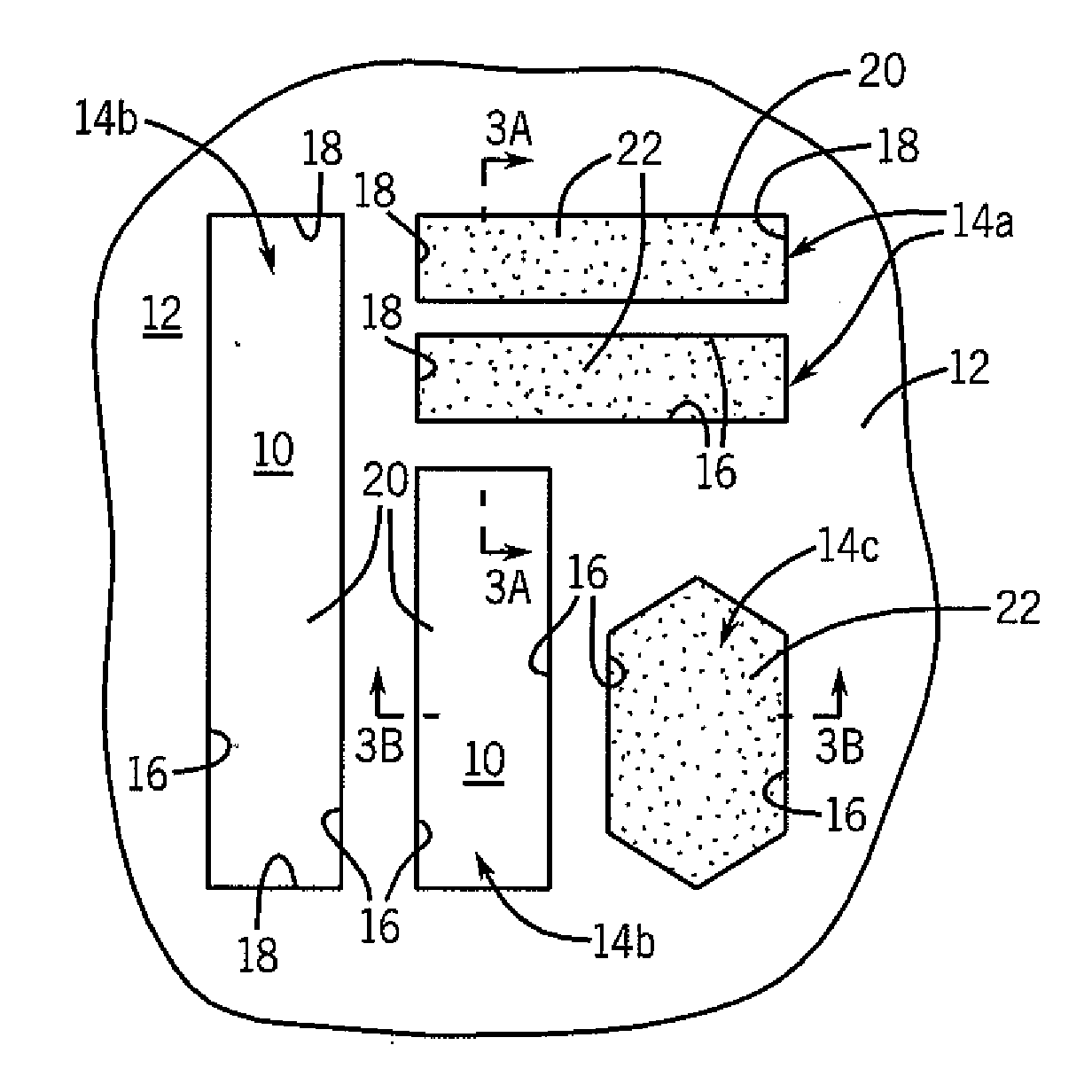
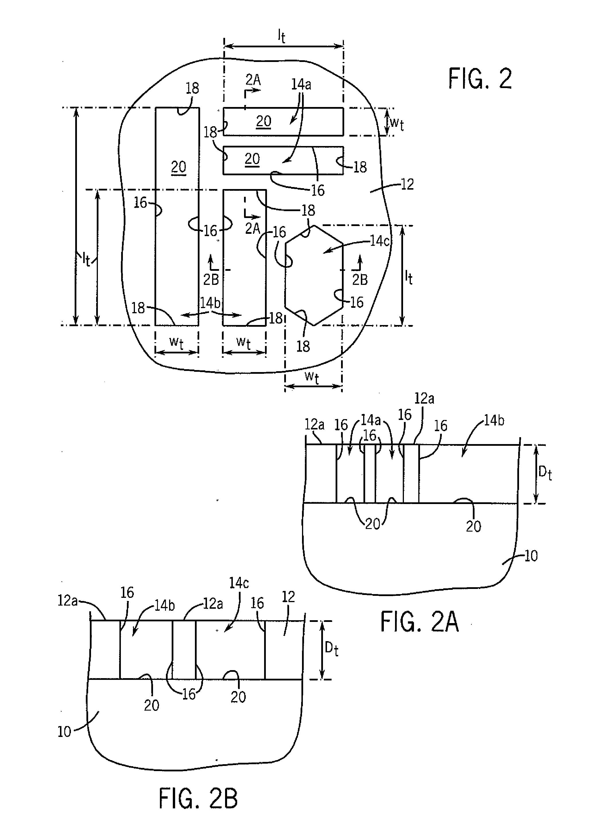
[0015]The following description with reference to the drawings provides illustrative examples of devices and methods according to embodiments of the invention. Such description is for illustrative purposes only and not for purposes of limiting the same.

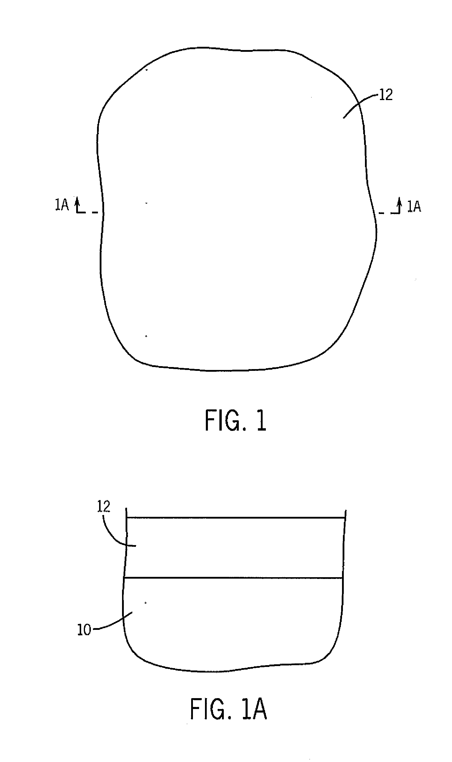
[0016]In the context of the current application, the term “semiconductor substrate” or “semiconductive substrate” or “semiconductive wafer fragment” or “wafer fragment” or “wafer” will be understood to mean any construction comprising semiconductor material, including but not limited to bulk semiconductive materials such as a semiconductor wafer (either alone or in assemblies comprising other materials thereon), and semiconductive material layers (either alone or in assemblies comprising other materials). The term “substrate” refers to any supporting structure including, but not limited to, the semiconductive substrates, wafer fragments or wafers described above.

[0017]“Lo” is the inherent pitch (bulk period or repeat unit) of structur...


PUM

PropertyMeasurementUnit
Lengthaaaaaaaaaa
Widthaaaaaaaaaa
Surface roughnessaaaaaaaaaa

Abstract

Methods for fabricating sublithographic, nanoscale microstructures arrays including openings and linear microchannels utilizing self-assembling block copolymers, and films and devices formed from these methods are provided. In some embodiments, the films can be used as a template or mask to etch openings in an underlying material layer.

Description

TECHNICAL FIELD[0001]Embodiments of the invention relate to methods of fabricating nanostructures by use of thin films of self-assembling block copolymers, and devices resulting from those methods.BACKGROUND OF THE INVENTION[0002]As the development of nanoscale mechanical, electrical, chemical and biological devices and systems increases, new processes and materials are needed to fabricate nanoscale devices and components. Optical lithographic processing methods are not able to accommodate fabrication of structures and features at the nanometer level. The use of self assembling diblock copolymers presents another route to patterning at nanometer dimensions. Diblock copolymer films spontaneously assembly into periodic structures by microphase separation of the constituent polymer blocks after annealing, for example by thermal annealing above the glass transition temperature of the polymer or by solvent annealing, forming ordered domains at nanometer-scale dimensions. Following self a...

Claims


Application Information

Patent Timeline
IPC IPC(8): B05D3/10B32B3/22C23F1/02
CPCB81C1/00031B81C2201/0149B81C2201/0198B82Y30/00H01J37/02Y10T428/2438G03F7/265Y10T428/24149Y10T428/24Y10T428/24174G03F7/0002
Inventor MILLWARD, DAN B.WESTMORELAND, DONALDSANDHU, GURTEJ
Owner MICRON TECH INC
Why Eureka
Try Eureka