
Gapfill for metal contacts

a metal contact and gap filling technology, applied in the direction of semiconductor devices, semiconductor/solid-state device details, electrical apparatus, etc., can solve the problems of difficult to fill the contact hole without creating a void, small contact hole fabrication, and shrinking of the critical dimension in semiconductor processes

Inactive Publication Date: 2008-12-18
INFINEON TECH AG +2
View PDF16 Cites 65 Cited by
  • Summary
  • Abstract
  • Description
  • Claims
  • Application Information

AI Technical Summary

Benefits of technology

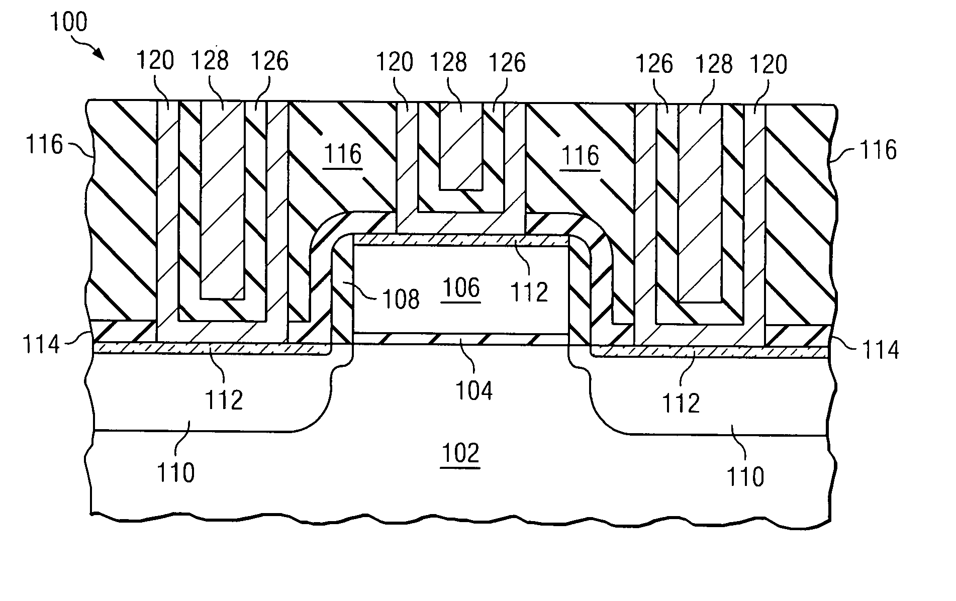
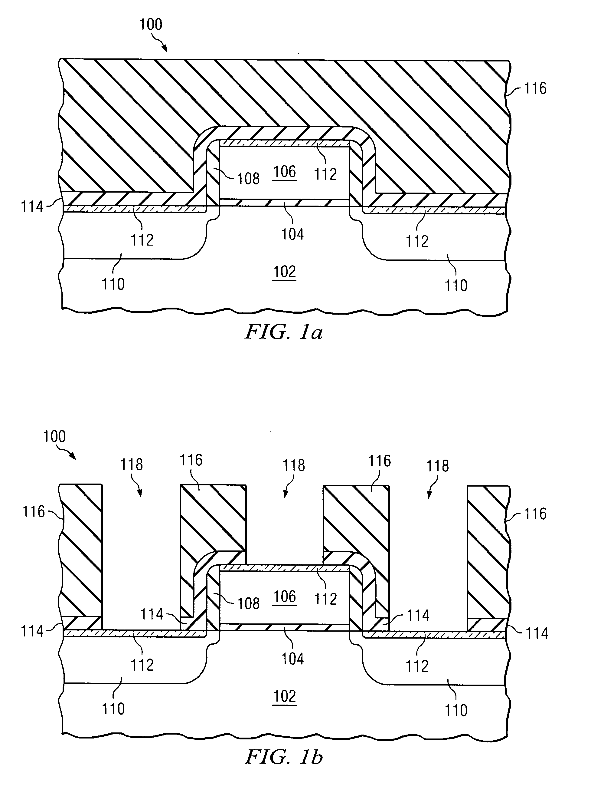
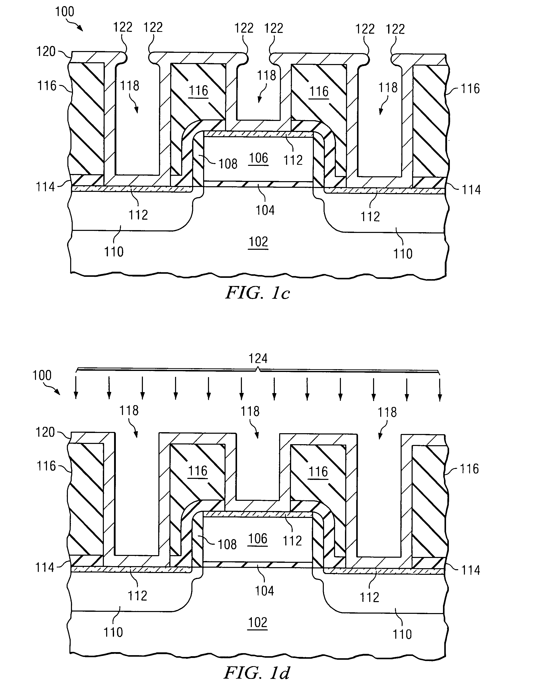
[0007]In one embodiment of the present invention, a method of making a semiconductor interconnect is provided. A contact hole is disposed in an insulating layer which is disposed on a semiconductor body. A first layer of metal is fabricated over the semiconductor body, a portion of which is disposed over a bottom and sidewalls of the contact hole. The first layer of metal is then thinned on the sidewalls of the contact hole, whereby the thickness of the first layer of metal on the sidewalls is made more uniform.

Problems solved by technology

One challenge is to effectively fabricate small contact holes.
The shrinking of the critical dimension in semiconductor processes poses a tough challenge for front end of the line (FEOL) metal fill processes.
Even with state of the art metal deposition processes, it is extremely difficult to fill the contact hole without creating a void.
During the subsequent chemical vapor deposition of tungsten, the top of the contact hole is prone to close before the entire contact is filled, thereby creating a void.
The presence of such a void poses potential device problems such as high contact resistance and blistering.
Often, during subsequent processing steps, slurries used in chemical-mechanical polishing (CMP) can get into the void causing vapor pressure to build up within the void during subsequent processing steps.

Method used


Image

  • Gapfill for metal contacts
  • Gapfill for metal contacts
  • Gapfill for metal contacts

Examples


Embodiment Construction

[0014]The making and using of preferred embodiments are discussed in detail below. It should be appreciated, however, that the present invention provides many applicable inventive concepts that may be embodied in a wide variety of specific contexts. The specific embodiments discussed are merely illustrative of specific ways to make and use the invention, and do not limit the scope of the invention.

[0015]The invention will now be described with respect to preferred embodiments in a specific context, namely a method for fabricating a semiconductor contact. Concepts of the invention can also be applied, however, to other electronic devices.

[0016]Referring first to FIG. 1a, which shows a cross section of the active area of device 100, a semiconductor body 102 is provided. A gate dielectric 104, a gate electrode 106, along with spacers 108 are formed over the semiconductor body 102.

[0017]The gate dielectric 104 may be deposited by chemical vapor deposition (CVD), thermally grown gate oxi...


PUM

PropertyMeasurementUnit
temperatureaaaaaaaaaa
poweraaaaaaaaaa

Abstract

A method of making a semiconductor interconnect is disclosed. A semiconductor body on which a transistor comprising a doped region is formed is provided. A dielectric region is formed over the doped region, and a contact hole is formed in the dielectric to expose the doped region. The contact hole is cleaned and a first layer of metal is formed over a bottom and sidewalls of the contact hole. The first layer of metal is thinned so that the thickness of the first layer of metal on the sidewalls is made more uniform. A barrier is formed over the first layer of metal and the contact hole is filled with conductive material.

Description

TECHNICAL FIELD[0001]This invention relates generally to semiconductor devices and methods, and more particularly to devices and methods for fabricating metal interconnects.BACKGROUND[0002]Semiconductor devices are used in a large number of electronic devices, such as computers, cell phones and others. One of the goals of the semiconductor industry is to continue shrinking the size and increasing the speed of individual devices. Smaller devices can operate at higher speeds since the physical distance between components is smaller. In addition, higher conductivity materials, such as copper, are replacing lower conductivity materials, such as aluminum. One challenge is to effectively fabricate small contact holes.[0003]The shrinking of the critical dimension in semiconductor processes poses a tough challenge for front end of the line (FEOL) metal fill processes. Contacts made at the FEOL portion of the semiconductor fabrication process are used to connect interconnect at the first lev...

Claims


Application Information

Patent Timeline
Patent Type & Authority Applications(United States)
IPC IPC(8): H01L21/4763H01L21/336
CPCH01L21/2855H01L21/76814H01L21/76846H01L21/76865H01L29/665H01L29/7833H01L23/485H01L21/28
Inventor HAMPP, ROLANDKWAK, JUN-KEUNWONG, KEITH KWONG HON
Owner INFINEON TECH AG
Learn More