Monitoring and control of integrated circuit device fabrication processes

a technology of integrated circuit devices and fabrication processes, applied in the direction of program control, total factory control, instruments, etc., can solve the problem that the fabrication process remains relatively difficult to monitor and control

Inactive Publication Date: 2008-12-18
PDF SOLUTIONS INC
View PDF31 Cites 83 Cited by
  • Summary
  • Abstract
  • Description
  • Claims
  • Application Information

AI Technical Summary

Problems solved by technology

However, fabrication processes remain relatively difficult to monitor and control due to their complexity and the large number of processing variables involved.

Method used


Image

  • Monitoring and control of integrated circuit device fabrication processes
  • Monitoring and control of integrated circuit device fabrication processes
  • Monitoring and control of integrated circuit device fabrication processes

Examples


Embodiment Construction

[0014]In the present disclosure, numerous specific details are provided, such as examples of apparatus, components, and methods, to provide a thorough understanding of embodiments of the invention. Persons of ordinary skill in the art will recognize, however, that the invention can be practiced without one or more of the specific details. In other instances, well-known details are not shown or described to avoid obscuring aspects of the invention.

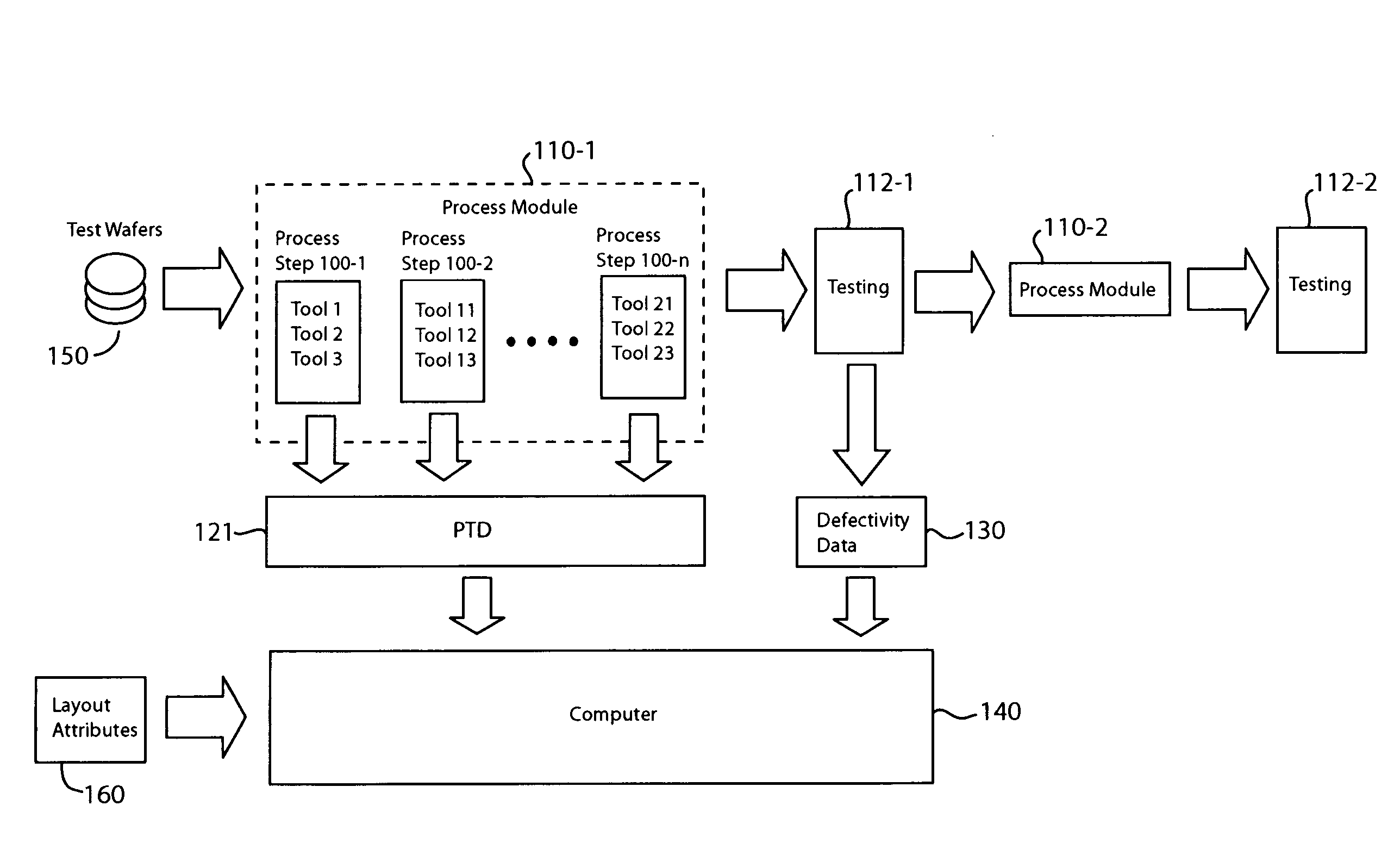
[0015]FIG. 1 shows a schematic diagram of a system for generating a yield impact model in accordance with an embodiment of the present invention. In the example of FIG. 1, a fabrication process may comprise one or more process modules 110 (i.e., 110-1, 110-2, . . . ), with each process module 110 comprising one or more process steps 100 (i.e., 100-1, 100-2, . . . ). A process module 110 may comprise a set of process steps 100 for fabricating a structure or region of the integrated circuit device. A process step 100 may be a chemical vapor d...


PUM


Abstract

An integrated circuit (IC) device fabrication process may be monitored by processing product wafers to fabricate product IC devices, collecting process tool data from tools used to fabricate the product IC devices, and testing the product IC devices. To predict and monitor yield, the process tool data collected during processing and the defectivity data from testing the product IC devices may be input to a yield model that also takes into account design information particular to the product devices. The design information may comprise layout attributes of the product devices. The yield model may be generated from a defectivity model created by processing test wafers to fabricate test structures, collecting process tool data from tools used to fabricate the test structures, and testing the test structures. The test structures may have varying layout attributes to cover a design space allowed by design rules for particular product IC devices.

Description

BACKGROUND OF THE INVENTION[0001]1. Field of the Invention[0002]The present invention relates generally to integrated circuit devices, and more particularly to integrated circuit device fabrication process control.[0003]2. Description of the Background Art[0004]Integrated circuit (IC) devices are generally fabricated on a substrate, such as a semiconductor wafer. The wafer is subjected to various fabrication processing steps to form dopant regions, dielectric layers, metal layers with metal lines, vias providing electrical connection between metal lines on different levels, trenches, and other regions and structures. The fabrication processing steps are generally well known and may include diffusion, implantation, deposition, electroplating, chemical-mechanical polishing (CMP), annealing, lithography, and etching, for example. The fabrication processing steps result in an integrated circuit device formed in one or more levels of the wafer. Several integrated circuit devices are typi...

Claims


Application Information

Patent Timeline
Patent Type & Authority Applications(United States)
IPC IPC(8): G06F19/00
CPCG05B19/41875G05B2219/32187G05B2219/32188G05B2219/32194Y02P90/02Y02P90/80
Inventor YU, GUANYUAN M.WILLIAMSON, MICHAEL V.GRAVES, SPENCER B.
Owner PDF SOLUTIONS INC
Why Eureka
Try Eureka