
Antenna, antenna apparatus, and communication device

Inactive Publication Date: 2008-12-25
HITACHI METALS LTD
View PDF4 Cites 23 Cited by
  • Summary
  • Abstract
  • Description
  • Claims
  • Application Information

AI Technical Summary

Benefits of technology

[0011]An advantage of the present invention is that a built-in antenna, an antenna apparatus, and communication device which uses the antenna apparatus is provided which is suited for an efficient mounting in a housing of a portable communication device, for achieving a very wide band in a high frequency band, and realizing a multi-band.
[0012]According to one aspect of the present invention, there is provided an antenna comprising a first antenna element including a base and a conductor penetrating through the base, and a second antenna element including a conductor portion having a shape of a plate or a line and a connecting conductor. A first end of the conductor of the first antenna element is connected to the connecting conductor of the second antenna element, and the connecting conductor of the second antenna element is connected to a partway on the conductor portion of the second antenna element. In this structure, the antenna comprises a conductor portion and a base. Because the conductor portion is formed extending along two directions with different lengths from a connection point with the connecting conductor, resonances can be achieved corresponding to approximately λ / 4 of two frequencies corresponding to the lengths of extension in the directions. In this structure, the second antenna element could correspond to the lower frequency band such as the GSM band with the first antenna element having the base. For example, when the antenna of the present invention is used in a low frequency band such as the GSM band used in the portable communication device, by providing the conductor portions in two directions with different lengths from the connection point with the connecting conductor, two resonance frequencies which slightly differ from each other can be realized. As a result, a low VSWR and a high gain can be obtained for a wider frequency band compared to a structure with only one resonance frequency, and a superior antenna characteristic can be achieved over a wide band. In addition, the base used in the first antenna element is not limited to a magnetic material ceramics, and an insulating material such as a dielectric ceramics may be used, which contributes to reduction in size and widening of the band. Because a line-shaped conductor is used as the conductor in the base and the conductor penetrates through the base, a stray capacity tends to not be formed, and the magnetic material portion can effectively function as an inductance component.

Problems solved by technology

As a result, the band width is narrowed, and it becomes difficult to apply the device for usage such as a quad-band portable phone which requires a very wide band.
However, in a communication device, in particular, in a portable communication device, because a mounting space of electronic components forming the antenna is limited, the mounting space of the antenna must be further reduced.
In addition, there had been a problem in that the gain reduction is large in the frequency band, in particular, in a low frequency side, used in the portable communication device in a structure with only a chip antenna which is formed with a dielectric ceramics or a magnetic material ceramics and a conductor provided within the ceramics.
In addition, although the use of the antenna element in which the dielectric ceramics or the magnetic material ceramics is combined with the conductor achieves a high gain in a particular frequency range within the band, a uniform high gain cannot be obtained over a range from a low frequency band to a high frequency band used in the portable communication device.
In particular, there had been problems in that the antenna element is not suited for use such as a portable communication device corresponding to the quad-band which requires realization of a low VSWR and a high gain over a very wide band, in particular, in the high frequency band.

Method used


Image

  • Antenna, antenna apparatus, and communication device
  • Antenna, antenna apparatus, and communication device
  • Antenna, antenna apparatus, and communication device

Examples


Embodiment Construction

[0048]A preferred embodiment of the present invention will now be described with reference to the drawings. In the following description, the same reference numerals are assigned to the same members.

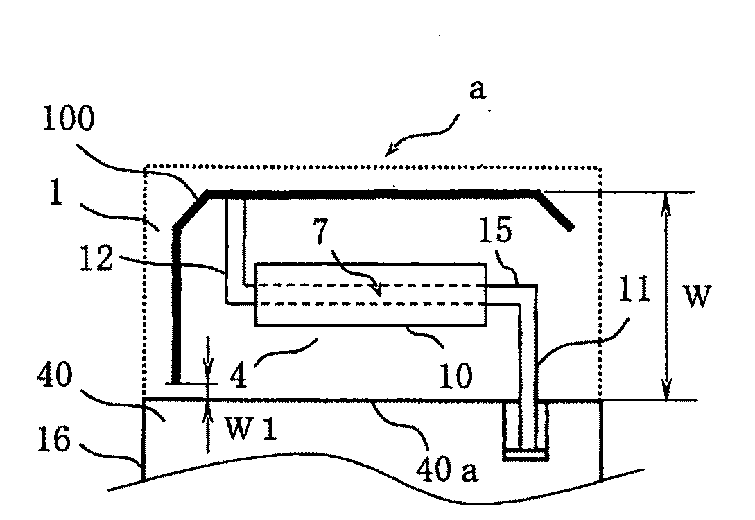
[0049]FIG. 1 shows one aspect of an antenna of a preferred embodiment according to the present invention. An antenna a of FIG. 1 is an antenna having a base (a magnetic material chip or a dielectric chip) and a conductor portion. The antenna can be mounted on a board and used. FIG. 1 is a plan view (which corresponds to a diagram of a board surface viewed from the above when the antenna is mounted on the board) of an antenna of the preferred embodiment.

[0050]As shown in FIG. 1, the antenna of the present embodiment comprises a first antenna element 4 having a first base 10 and a conductor 7 which is provided within the base 10, and a second antenna element 1 having a plate-shaped conductor portion 100 and a connecting conductor 12. The connecting conductor 12 is connected to a partway on...


PUM


Abstract

An antenna is provided which includes a first antenna element having at least one base and a conductor penetrating through the base and a second antenna element having a conductor portion having a shape of a plate or a line and a connecting conductor, wherein a first end of the conductor of the first antenna element is connected to the connecting conductor of the second antenna element, and the connecting conductor of the second antenna element is connected to a partway on the conductor portion of the second antenna element.

Description

[0001]The applications, from which priority are claimed, are incorporated herein by reference.BACKGROUND OF THE INVENTION[0002]1. Field of the Invention[0003]The present invention relates to an antenna which is used in an electronic device having a communication function, for example, a communication device such as a portable phone and a portable terminal device, and further to an antenna apparatus and a communication device which use the antenna.[0004]2. Related Art[0005]A communication device such as a portable phone and a wireless LAN has a usage frequency band of several hundreds of MHz to few GHz, and a high gain and a high efficiency in the band are desired. Therefore, an antenna which is used in the communication device is required to function with a high gain in the band, and, in addition, is also required to have a small size and a low height due to its usage form. Moreover, in recent years, there is a growing demand for handling, with one portable phone, 4 bands including ...

Claims


Application Information

Patent Timeline
IPC IPC(8): H01Q1/38
CPCH01Q1/38H01Q9/30H01Q9/40
Inventor AOYAMA, HIROYUKIGONDA, MASAYUKI
Owner HITACHI METALS LTD
Learn More