

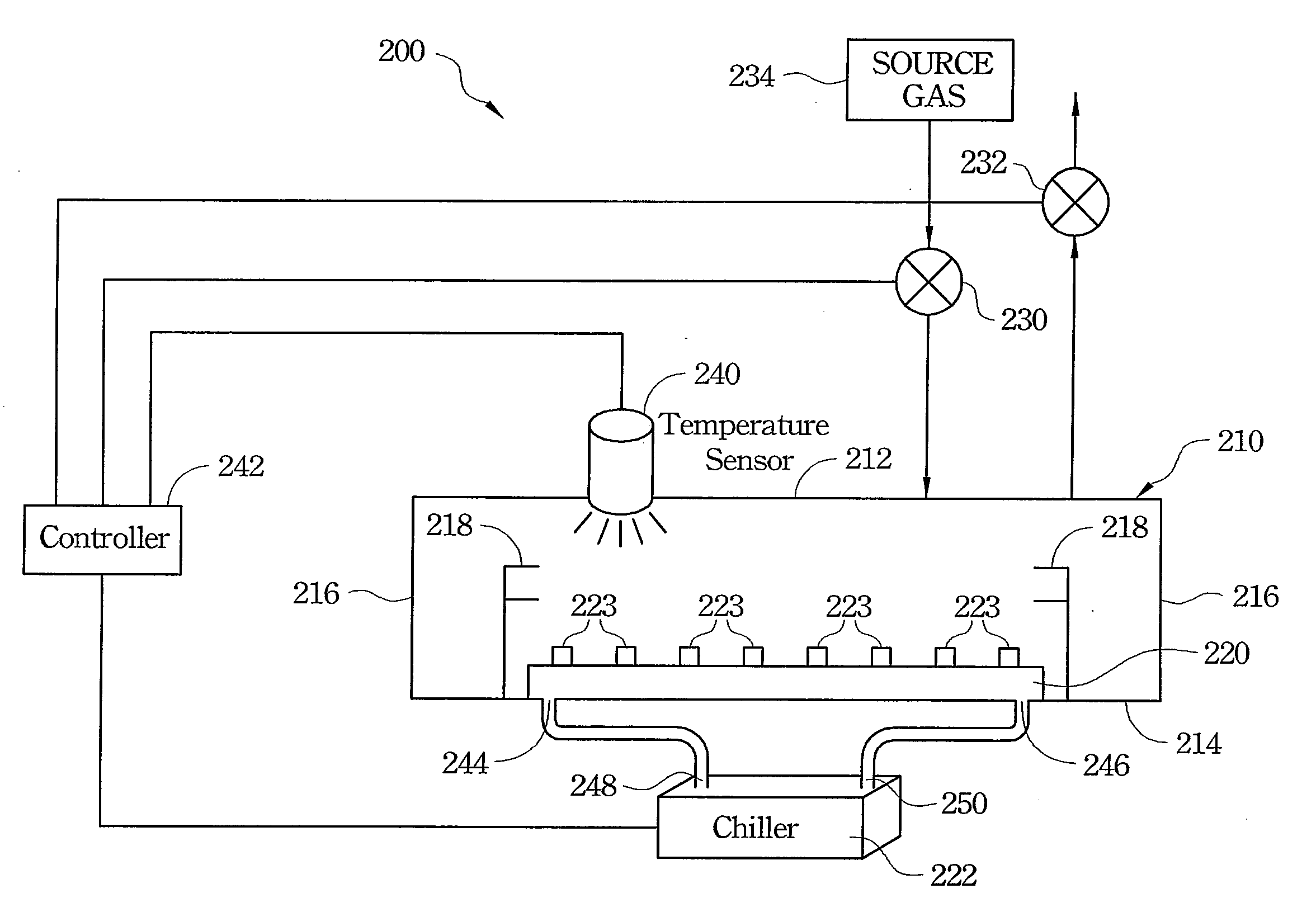
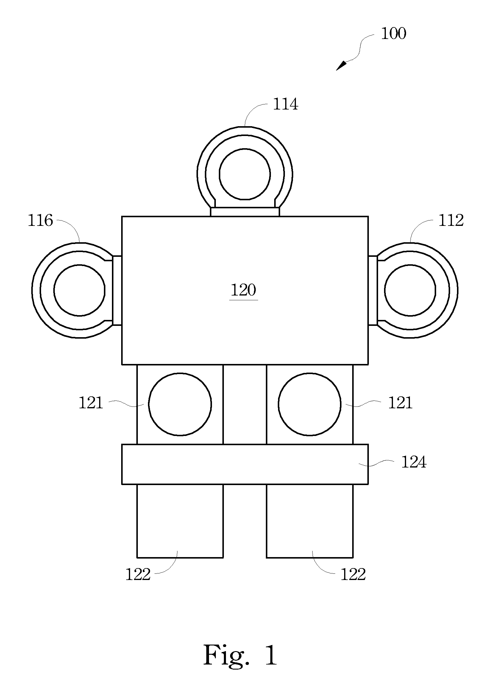
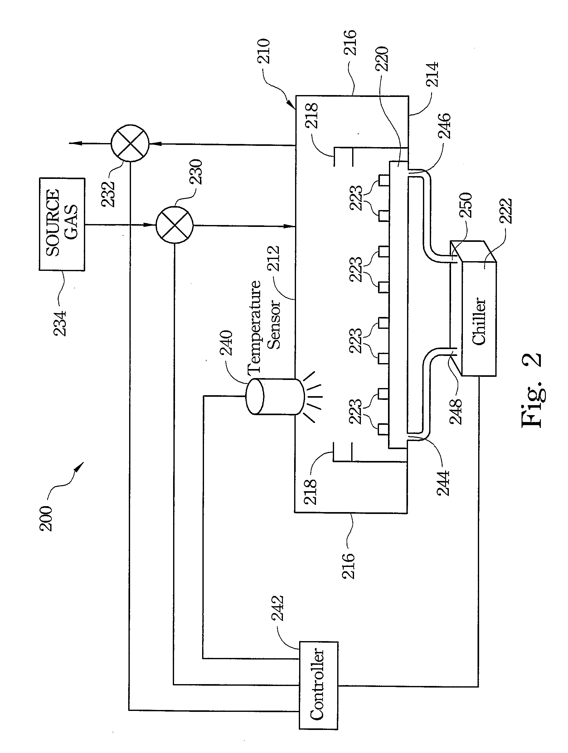
Temperature Controlled Loadlock Chamber
- Summary
- Abstract
- Description
- Claims
- Application Information
AI Technical Summary
Benefits of technology
Problems solved by technology
Method used
Image

Examples
Embodiment Construction
[0017]The operation and fabrication of the presently preferred embodiments are discussed in detail below. However, the embodiments and examples described herein are not the only applications or uses contemplated for the invention. The specific embodiments discussed are merely illustrative of specific ways to make and use the invention, and do not limit the scope of the invention or the appended claims.
[0018]Exemplary structures and methods are provided below for fabricating a metal oxide semiconductor field effect transistor (MOSFET) according to embodiments of the invention. Although the exemplary embodiments are described as a series of steps, it will be appreciated that this is for illustration and not for the purpose of limitation. For example, some steps may occur in a different order than illustrated yet remain within the scope of the invention. In addition, not all illustrated steps may be required to implement the present invention. Furthermore, the structures and methods ac...
PUM
 Abstract
Description
Claims
Application Information