Liquid crystal display device

a liquid crystal display and display device technology, applied in semiconductor devices, instruments, optics, etc., can solve the problems of reducing the yield, increasing the cost, and increasing the risk of oxidation of the surface of a microcrystalline semiconductor film where crystal grains are exposed, and achieves high mass productivity and reliable electric characteristics

Inactive Publication Date: 2009-01-01
SEMICON ENERGY LAB CO LTD
View PDF70 Cites 133 Cited by
  • Summary
  • Abstract
  • Description
  • Claims
  • Application Information

AI Technical Summary

Benefits of technology

[0025]According to the present invention, it is possible to manufacture, with high mass productivity, li

Problems solved by technology

However, the process for crystallization of an amorphous semiconductor film provided over a glass substrate is more complex than that in the case of using an amorphous semiconductor film; accordingly, there are problems in that yield is decreased and cost is increased.
There is also a problem in that a surface of a microcrystalline semiconductor film

Method used


Image

  • Liquid crystal display device
  • Liquid crystal display device
  • Liquid crystal display device

Examples


embodiment mode 1

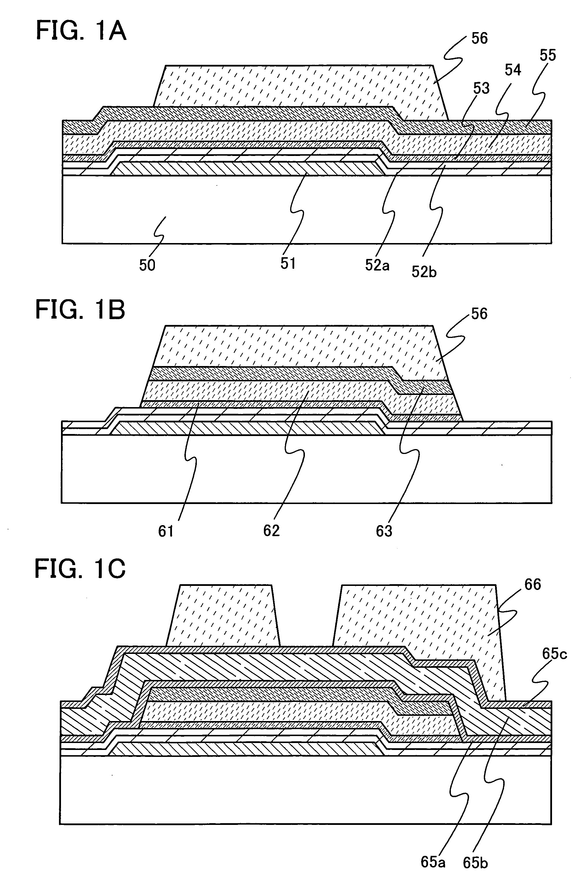
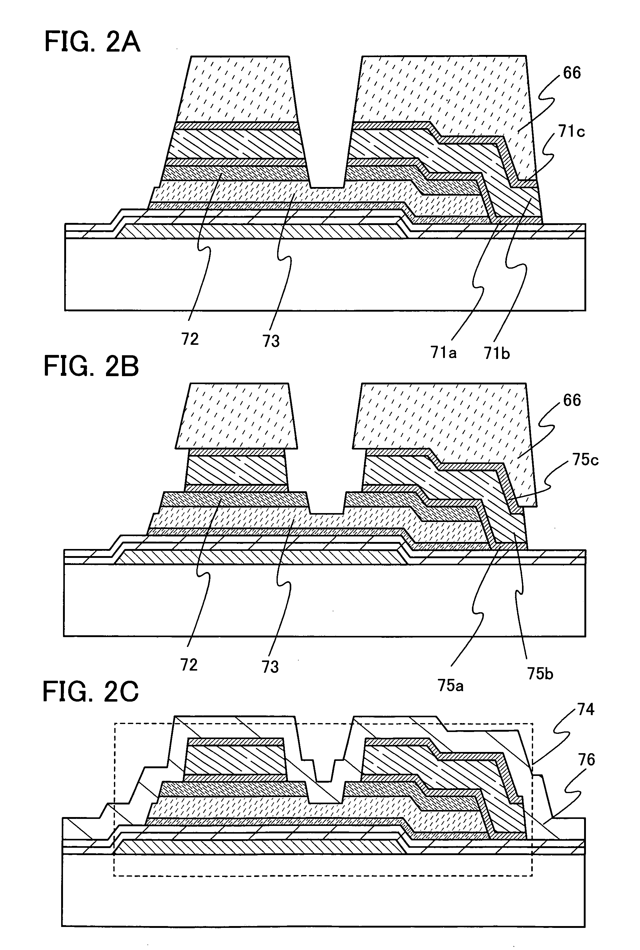
[0067]In this embodiment mode, manufacturing processes of thin film transistors used for a liquid crystal display device are described with reference to FIGS. 1A to 8D. FIGS. 1A to 3 and FIGS. 5A to 7 are cross-sectional views showing manufacturing processes of thin film transistors, and FIGS. 4A to 4C and FIGS. 8A to 8D are top views each showing a connection region of a thin film transistor and a pixel electrode in a single pixel.

[0068]A thin film transistor having a microcrystalline semiconductor film, which is of an n type, is more suitable for use in a driver circuit than that of a p type because it has a higher field-effect mobility. It is desired that all thin film transistors formed over the same substrate have the same polarity, in order to reduce the number of steps. Here, description is made using an n-channel thin film transistor.

[0069]As shown in FIG. 1A, a gate electrode 51 is formed over a substrate 50. As the substrate 50, any of the following substrates can be used:...

embodiment mode 2

[0154]In this embodiment mode, a liquid crystal display device including the thin film transistor described in Embodiment Mode 1 is described below.

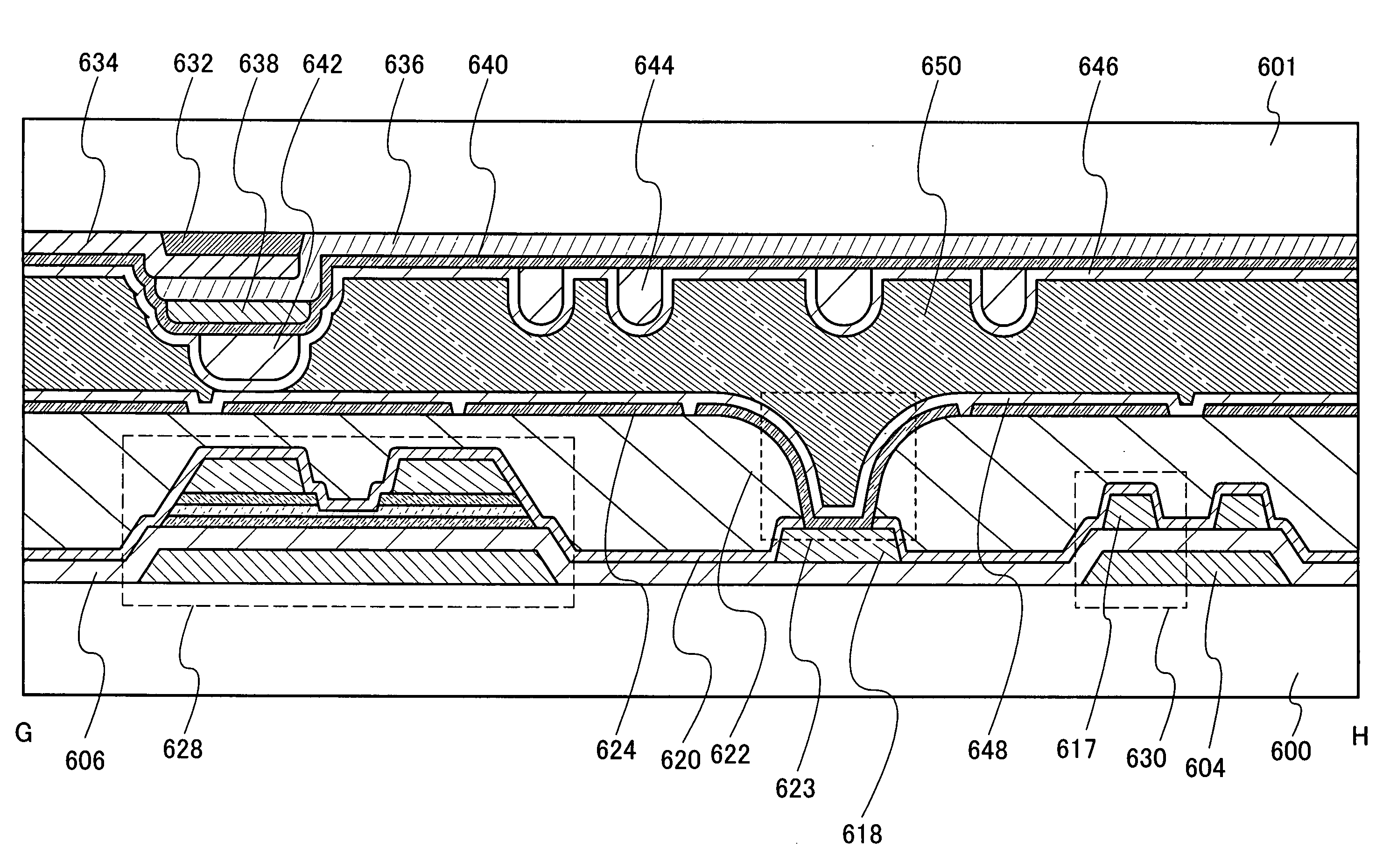
[0155]First, a vertical alignment (VA) liquid crystal display device is described. The VA liquid crystal display device is a kind of form in which alignment of liquid crystal molecules of a liquid crystal panel is controlled. The VA liquid crystal display device is a form in which liquid crystal molecules are vertical to a panel surface when voltage is not applied. In particular, in this embodiment mode, it is devised that a pixel is divided into several regions (sub-pixels) so that molecules are aligned in different directions in the respective regions. This is referred to as domain multiplication or multi-domain design. In the following description, a liquid crystal display device with multi-domain design is described.

[0156]FIGS. 14 and 15 show a pixel electrode and a counter electrode, respectively. FIG. 14 is a plan view of a side of...

embodiment mode 3

[0198]Next, a structure of a display panel, which is one mode of a liquid crystal display device of the present invention, is described below.

[0199]FIG. 10A shows a mode of a display panel in which a signal line driver circuit 6013 which is separately formed is connected to a pixel portion 6012 formed over a substrate 6011. The pixel portion 6012 and a scan line driver circuit 6014 are each formed using a thin film transistor in which a microcrystalline semiconductor film is used. When the signal line driver circuit is formed using a transistor in which higher field-effect mobility can be obtained compared with the thin film transistor in which the microcrystalline semiconductor film is used, an operation of the signal line driver circuit which demands higher driving frequency than that of the scan line driver circuit can be stabilized. Note that the signal line driver circuit 6013 may be formed using a transistor using a single crystalline semiconductor, a thin film transistor usin...


PUM


Abstract

An object is to propose a method of manufacturing, with high mass productivity, liquid crystal display devices having thin film transistors with highly reliable electric characteristics. In a liquid crystal display device having an inverted staggered thin film transistor, the inverted staggered thin film transistor is formed as follows: a gate insulating film is formed over a gate electrode; a microcrystalline semiconductor film which functions as a channel formation region is formed over the gate insulating film; a buffer layer is formed over the microcrystalline semiconductor film; a pair of source and drain regions are formed over the buffer layer; and a pair of source and drain electrodes are formed in contact with the source and drain regions so as to expose a part of the source and drain regions.

Description

BACKGROUND OF THE INVENTION[0001]1. Field of the Invention[0002]The present invention relates to a liquid crystal display device using a thin film transistor at least in a pixel portion.[0003]2. Description of the Related Art[0004]In recent years, techniques to form thin film transistors using a semiconductor thin film (with a thickness of approximately several tens to several hundreds of nanometers) which is formed over a substrate having an insulating surface have attracted attention. Thin film transistors are widely used in electronic devices such as ICs and electro-optical devices, and their development especially as switching elements for image display devices has been accelerated.[0005]As a switching element of an image display device, a thin film transistor using an amorphous semiconductor film, a thin film transistor using a polycrystalline semiconductor film, or the like is used. As a method of forming a polycrystalline semiconductor film, there is known a technique in whic...

Claims


Application Information

Patent Timeline
IPC IPC(8): G02F1/136
CPCH01L21/67207G02F1/1368G02F1/133345H01L29/41733H01L29/66765H01L29/78678H01L29/78696H01L29/04H01L29/458H01L29/78618
Inventor YAMAZAKI, SHUNPEISUZUKI, YUKIEKUWABRARA, HIDEAKIKIMURA, HAJIMEMIYAIRI, HIDEKAZUKUROKAWA, YOSHIYUKIKOBAYASHI, SATOSHI
Owner SEMICON ENERGY LAB CO LTD
Why Eureka
Try Eureka