Package for micromirror device

Active Publication Date: 2009-01-08
IGNITE INC
View PDF41 Cites 29 Cited by
  • Summary
  • Abstract
  • Description
  • Claims
  • Application Information

AI Technical Summary

Benefits of technology

[0048]The present invention discloses a package for a mirror device to improve the efficiency of heat dissipation through heat conduction, convection and radiation.
[0049]This invention also discloses a projection apparatus using a mirror device accommodated by the package with improved

Problems solved by technology

This in turn limits the number of units of device substrates that are cut out of one semiconductor wafer, increasing the cost of the device substrate.
Furthermore, if the number of units of device substrate that are cut out of a semiconductor wafer is limited, the ratio of defective units to the number of usable units is increased making it difficult to improve the yield in production.
The processes for manufacturing a package with metallic c

Method used


Image

  • Package for micromirror device
  • Package for micromirror device
  • Package for micromirror device

Examples


embodiment 1-1

[0087]The following description explains the configuration of a package according to a preferred embodiment 1-1 of the present invention.

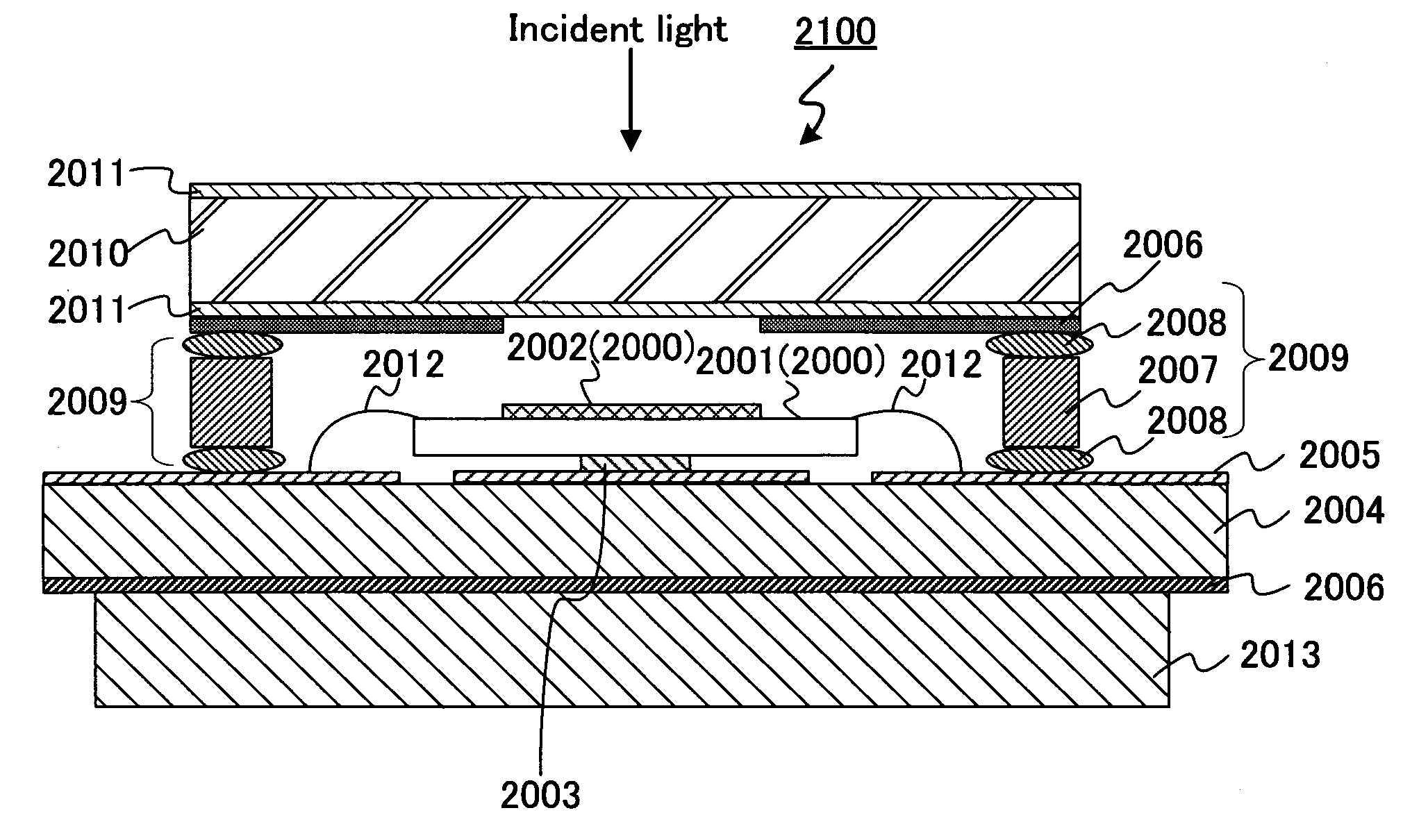
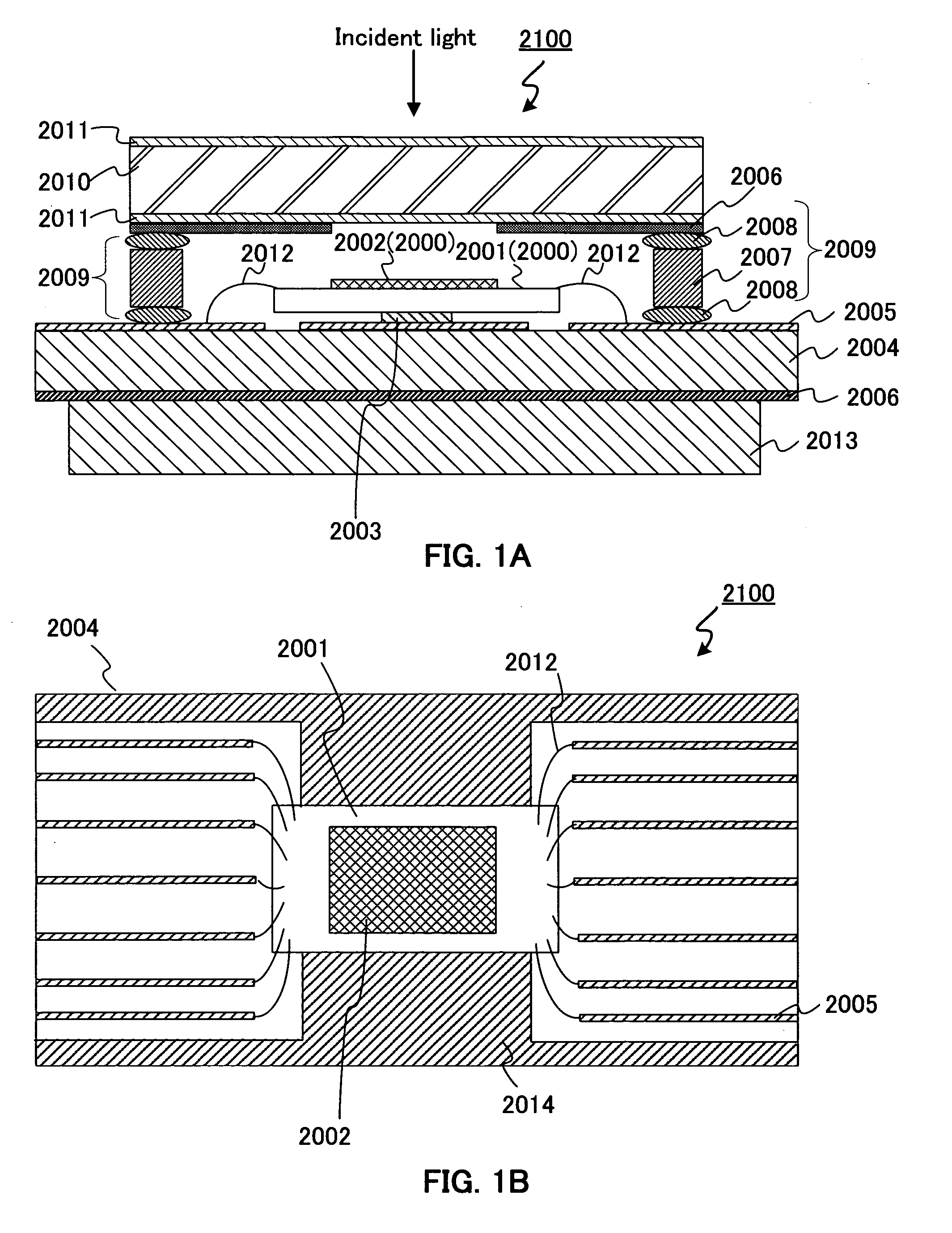
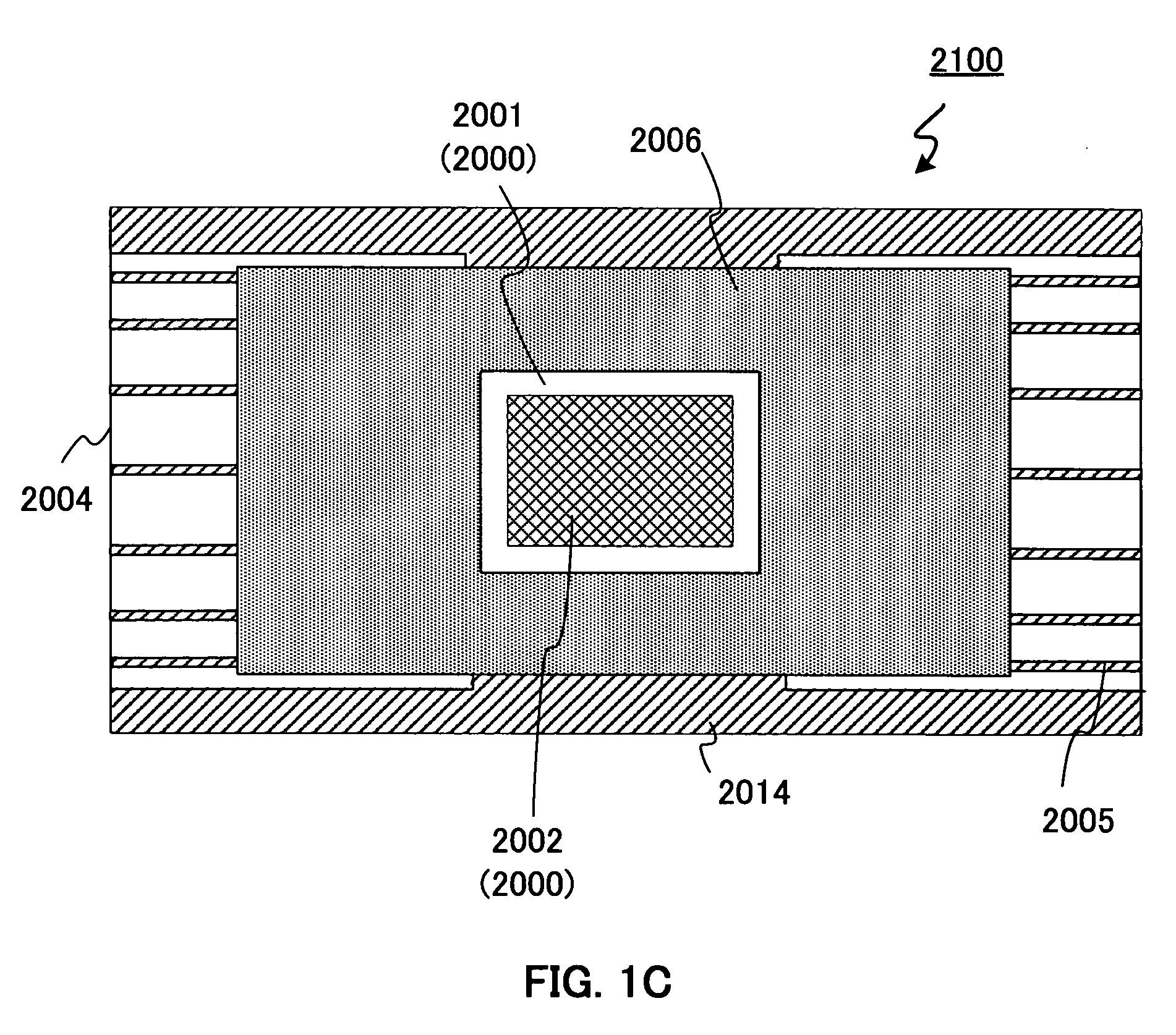
[0088]FIGS. 1A through 1E show the assembly 2100 that contains the mirror device 2000 in a glass package. The mirror device 2000 corresponds to the spatial light modulator 5100 described later. FIG. 1A is a front cross-sectional diagram of the assembly 2100 that contains and protects the mirror device 2000 in a glass package.

[0089]The assembly 2100 includes a package substrate 2004 made of a glass material, a cooling / radiation member (heat sink) 2013, an intermediate member 2009, a thermal conduction member 2003, a mirror device 2000 and a cover glass 2010. Here, the “package” generally refers to the parts assembled together as a container unit for containing and protecting the mirror device 2000. As an example, the package substrate 2004 formed with glass material, cooling / radiation member (heat sink) 2013, intermediate member 2009, thermal conduc...

embodiment 1-2

[0162]A package according to a preferred embodiment 1-2 is an exemplary modification of that of embodiment 1-1.

[0163]The package according to the embodiment 1-2 is configured to have a separate package substrate, or to have an opening part in the package substrate, which is the different from the package according to the embodiment 1-1. Further, the package improves the efficiency heat dissipation by placing the opening part of the package substrate under the mirror device. In this case, a seal member similar to the intermediate member is placed between the device substrate and package substrate for joining them together, and thereby, a contact between the inside and outside of the package is removed.

[0164]Further, it is possible to transmit the heat out from the package directly from the device substrate by way of a thermal conduction member connecting it to the bottom surface of the device substrate of the mirror device. Therefore, an alternative configuration may be provide by el...

embodiment 1-3

[0173]A package according to a preferred embodiment 1-3 of the present invention is another exemplary modification of the package according to the embodiment 1-1.

[0174]The package according to the embodiment 1-3 differs from the package of the embodiment 1-1. The package substrate is composed of a glass material; a device substrate is composed of a silicon material, a metallic material or a ceramic material. The package substrate includes a cavity, and is configured to form an electrical connection between a device substrate and a cover glass by forming a circuit-wiring pattern on the cover glass.

[0175]FIG. 3 is a front cross-sectional diagram of an assembly body 2300 that packages a mirror device 2000 to electrically connect to a device substrate 2001 by forming a cover glass 2010 with a circuit-wiring pattern 2005 using a support substrate 2019.

[0176]The assembly body 2300 shown in FIG. 3 is configured to form a light shield layer 2006 on the top surface of the cover glass 2010 an...


PUM


Abstract

The present invention discloses a mirror device that includes a mirror element which further comprising an elastic hinge and a mirror and which modulates incident light emitted from a light source, a device substrate on which a drive circuit for driving the mirror element is placed, a package substrate which is made of transparent glass or a silicon material and on which the device substrate is placed, a metallic thermal transfer path connected to the device substrate, and a cover glass connected to the package substrate so that the device substrate is covered.

Description

[0001]This is a Non-provisional application of a pending U.S. Patent Provisional Application No. 60 / 967,811 filed on Sep. 6, 2007. The Patent Application 60 / 967,811 is a Continuation In Part (CIP) Application of a pending U.S. patent application Ser. No. 11 / 121,543 filed on May 3, 2005 issued into U.S. Pat. No. 7,268,932. The application Ser. No. 11 / 121,543 is a Continuation In Part (CIP) Application of three previously filed applications. These three applications are Ser. Nos. 10 / 698,620 filed on Nov. 1, 2003, 10 / 699,140 filed on Nov. 1, 2003 now issued into U.S. Pat. No. 6,862,127, and Ser. No. 10 / 699,143 filed on Nov. 1, 2003 now issued into U.S. Pat. No. 6,903,860 by the Applicant of this patent applications. The disclosures made in these patent applications are hereby incorporated by reference in this patent application.BACKGROUND OF THE INVENTION[0002]1. Field of the Invention[0003]The present invention relates generally to the image projection apparatuses manufactured by appl...

Claims


Application Information

Patent Timeline
IPC IPC(8): H01L33/00
CPCG02B26/0841H01L2224/48091H01L2924/16195H01L2924/00014
Inventor MAEDA, YOSHIHIRONISHINO, HIROKAZUSHIRAI, AKIRAICHIKAWA, HIROTOSHIISHII, FUSAO
Owner IGNITE INC
Why Eureka
Try Eureka