Avalanche photodiode detector
a photodiode detector and photodiode technology, applied in the field of photodiode detectors, can solve the problems of reducing the overall quantum efficiency, and after pulsing performance of an apd, and the multiplication layer does not provide flexibility in selecting different materials
- Summary
- Abstract
- Description
- Claims
- Application Information
AI Technical Summary
Benefits of technology
Problems solved by technology
Method used
Image
Examples
Embodiment Construction
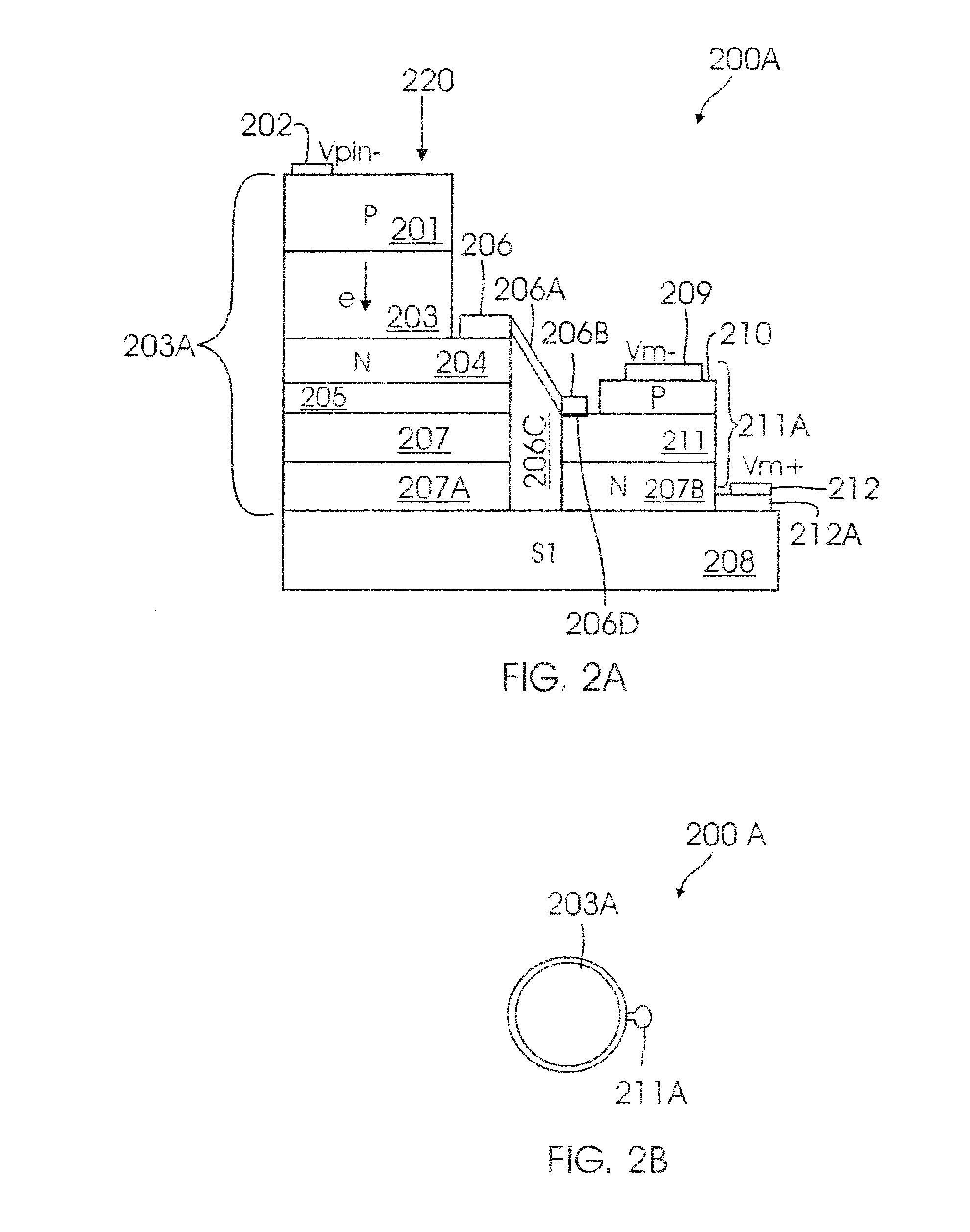
[0021]In one aspect of the present embodiments, a three terminal APD structure with separate absorption and multiplication layers (also referred to as “TT-SAM APD or APD”) is provided. The absorption layer and multiplication layer may be grown separately and hence are controlled independently. This allows one to select different materials for the absorption and multiplication layer. The APD of the present embodiments also provides an additional terminal. The additional terminal enables individual control of bias across an absorption (Absorber”) region and a multiplication (“Multiplier”) region.
[0022]To facilitate an understanding of APD structure, a general overview of a conventional APD structure will be described. The specific structural components and layers of the present embodiments will then be described with reference to the general structure of APD.
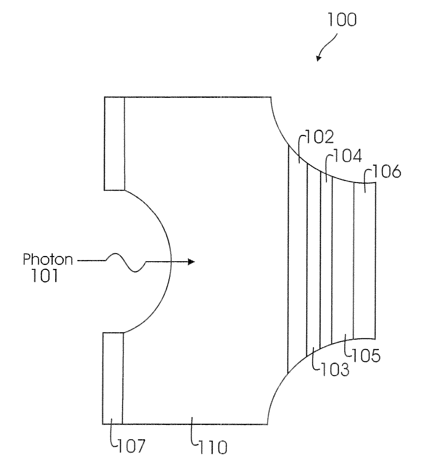
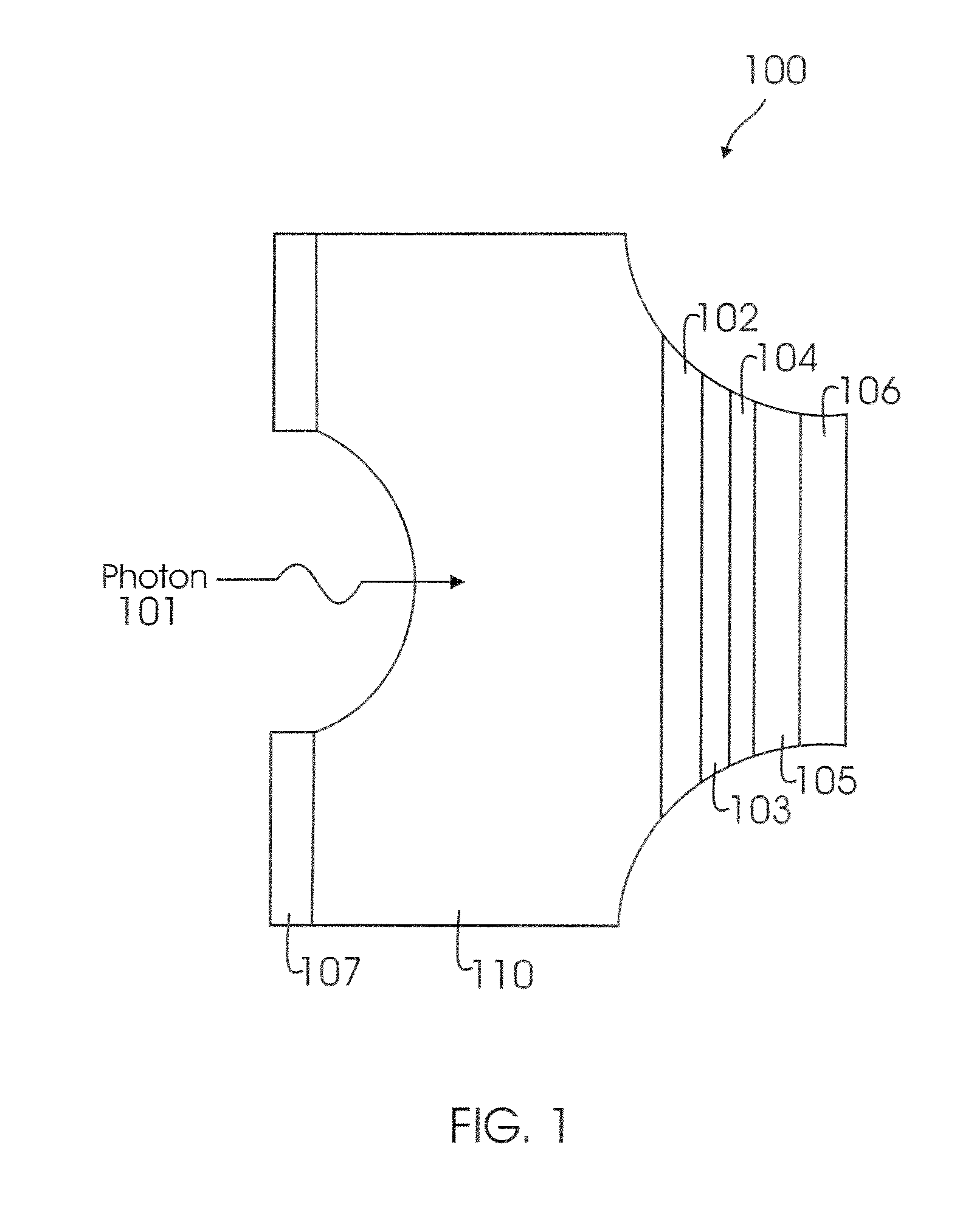
[0023]FIG. 1 shows a top level block diagram of a conventional APD structure. APD 100 Includes a P-InP substrate layer 110; a P-...
PUM
 Abstract
Description
Claims
Application Information


