Thickness Indicators for Wafer Thinning

Inactive Publication Date: 2009-01-08
TAIWAN SEMICON MFG CO LTD
View PDF6 Cites 56 Cited by
  • Summary
  • Abstract
  • Description
  • Claims
  • Application Information

AI Technical Summary

Benefits of technology

[0021]An advantage of a preferred embodiment of the present invention is that the coarse grinding may be accomplished with greater accuracy to the appropriate level without the physical limitations found in the mechanical thickness dial.
[0022]A further ad

Problems solved by technology

Such thickness requirements may risk damage to the active device layer if the mechanism to determine material thickness during the backside grinding process is not accurate.
However, because the dial gauge itself is a mechanical process, its accuracy is intrinsically limited. FIGS. 1A-1C are cross-sectional diagrams illustrating a typical wafer grinding process.
Because the grinding process provides such a coarse grinding mechanism, the top most layer of Si of stacked wafer 12 is typically damaged, which generally prompts additional fine polishing to finish out the proce

Method used


Image

  • Thickness Indicators for Wafer Thinning
  • Thickness Indicators for Wafer Thinning
  • Thickness Indicators for Wafer Thinning

Examples


Example

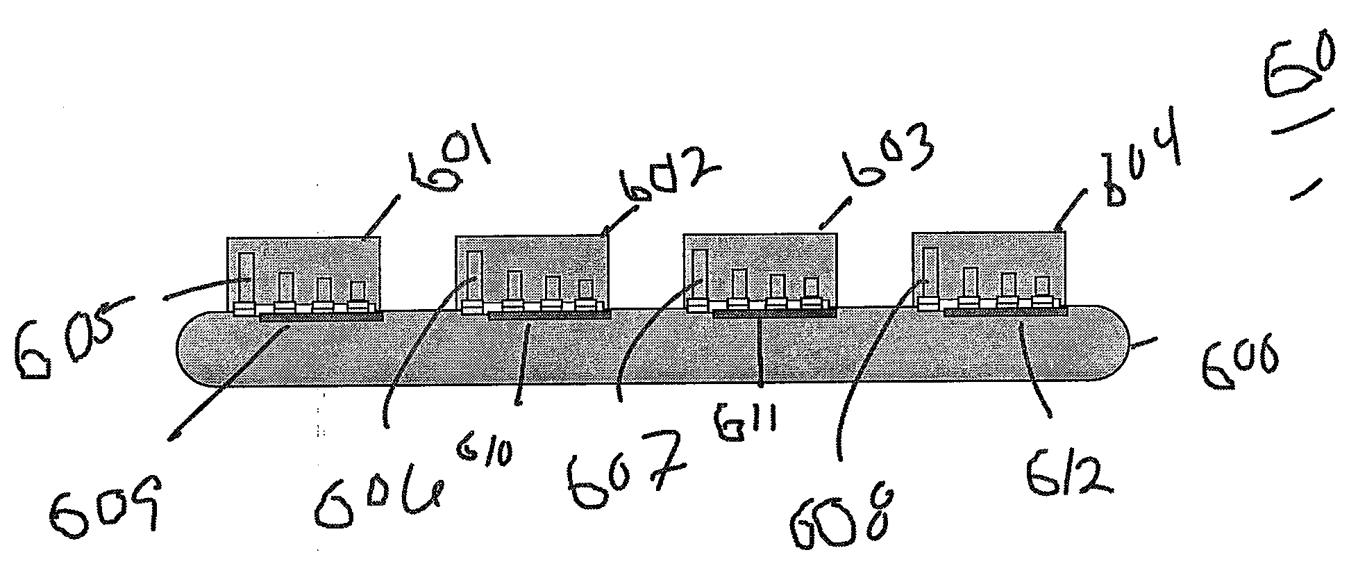
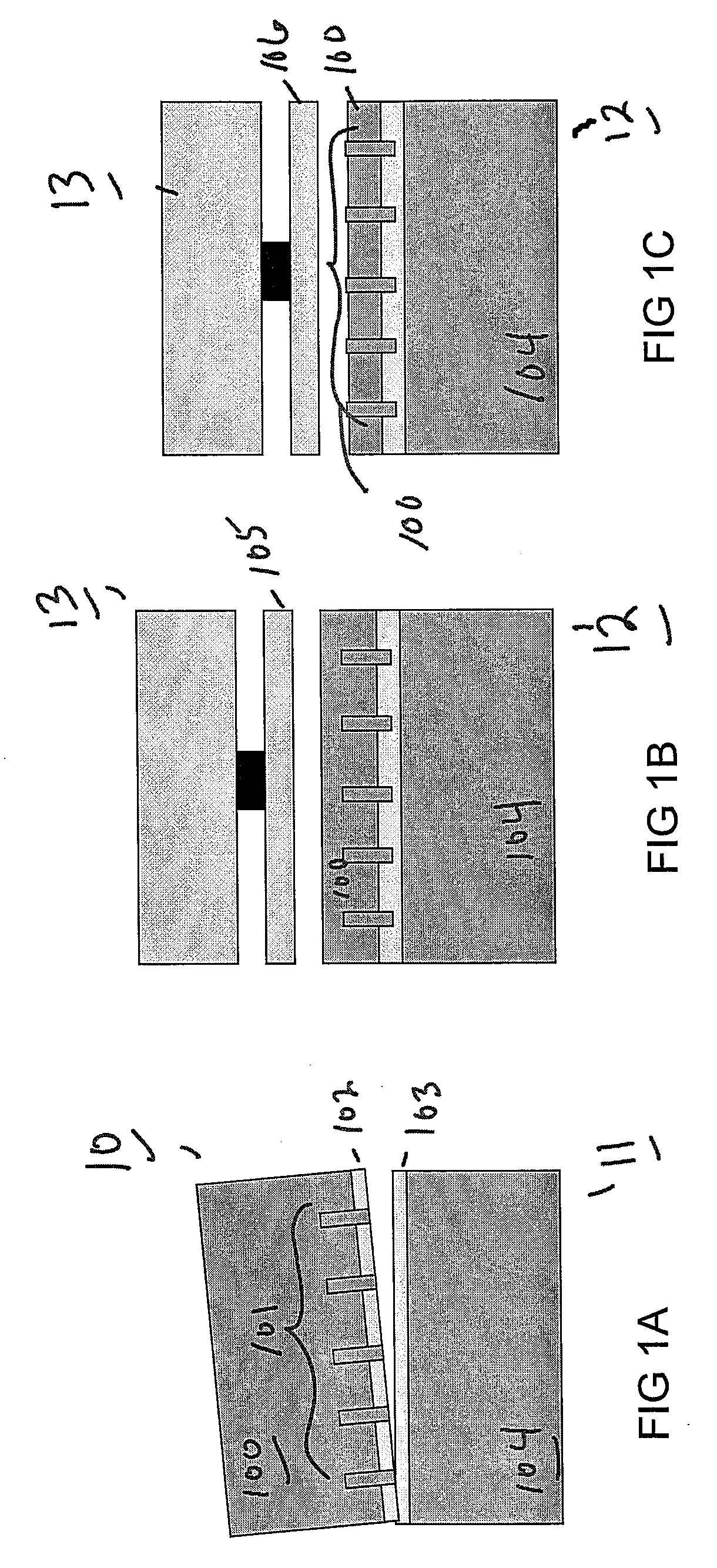
[0035]The making and using of the presently preferred embodiments are discussed in detail below. It should be appreciated, however, that the present invention provides many applicable inventive concepts that can be embodied in a wide variety of specific contexts. The specific embodiments discussed are merely illustrative of specific ways to make and use the invention, and do not limit the scope of the invention.

[0036]The present invention will be described with respect to preferred embodiments in a specific context, namely a two-layer 3D IC semiconductor device with TSV formed as the thickness indicator. The invention may also be applied, however, to various other multilayer semiconductor devices, and the thickness indicators may be any type of device structure, such as trenches, TSV, alignment marks, combinations thereof, and the like.

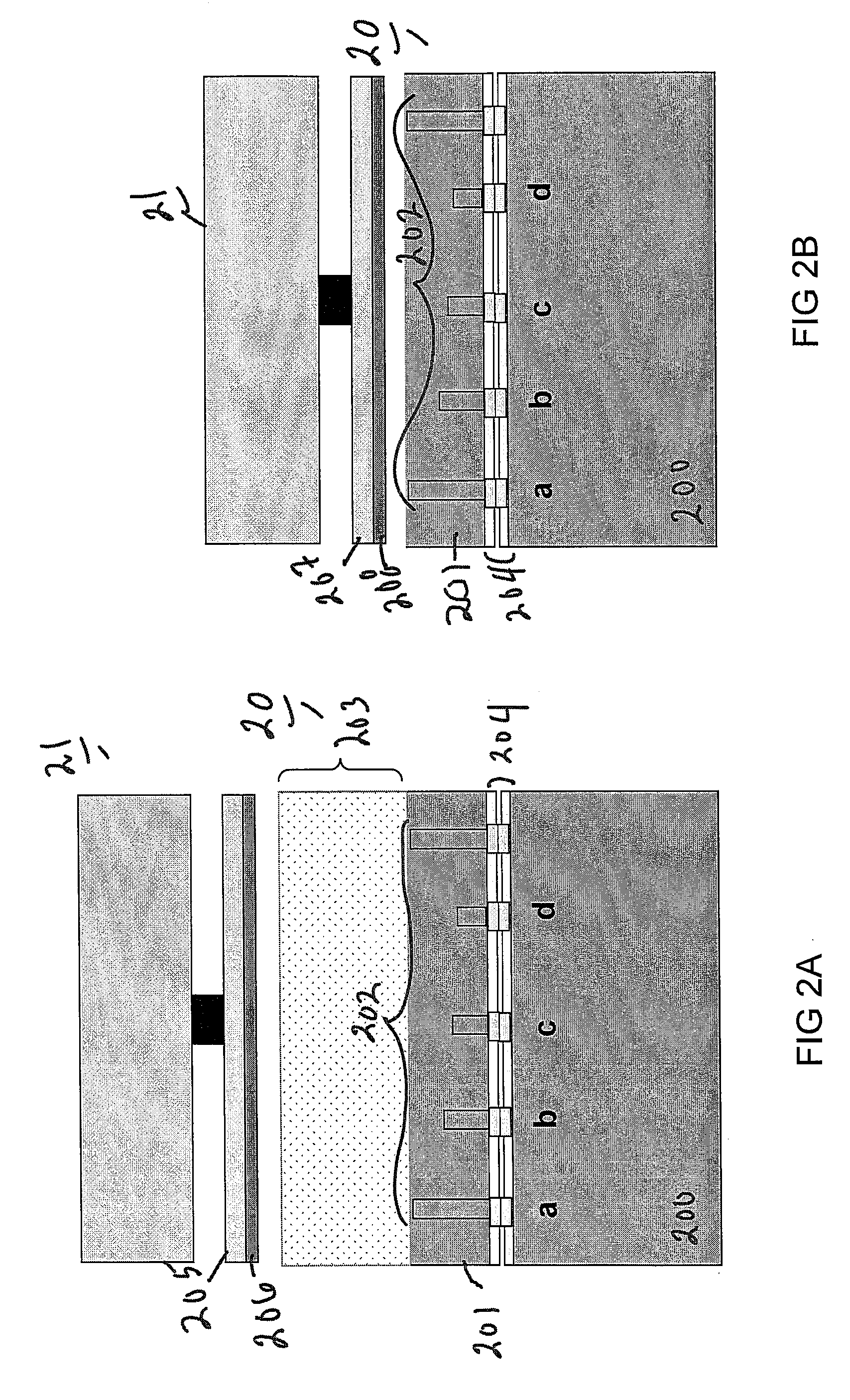
[0037]With reference now to FIG. 2A, there is shown a cross-sectional view of stacked wafer 20 during a thinning process configured according to one ...


PUM


Abstract

A wafer thinning system and method are disclosed that includes grinding away substrate material from a backside of a semiconductor device. A current change is detected in a grinding device responsive to exposure of a first set of device structures through the substrate material, where the grinding is stopped in response to the detected current change. Polishing repairs the surface and continues to remove an additional amount of the substrate material. Exposure of one or more additional sets of device structures through the substrate material is monitored to determine the additional amount of substrate material to remove, where the additional sets of device structures are located in the semiconductor device at a known depth different than the first set.

Description

TECHNICAL FIELD[0001]The present invention relates, in general, to semiconductor wafer thinning, and, more particularly, to thickness indicators used for assisting the wafer thinning process.BACKGROUND[0002]A semiconductor wafer generally includes a first or “front” side having integrated circuits formed thereon, and a backside comprising a thickness of a semiconductor material (e.g., silicon (Si), gallium arsenide (GaAs), or the like) either in a bulk Si / semiconductor wafer or a Si / semiconductor on insulator (SOI) package. Prior to the dicing and packaging of the individual integrated circuit chips, the backside of the wafer is typically thinned to remove unwanted semiconductor material.[0003]There are several different bonding and wafer thinning processes that are currently used depending on the type of semiconductor substrate (e.g., SOI vs. bulk Si) or on the point in the process at which via are formed (i.e., before or after bonding). When using SOI substrates, the typical proce...

Claims


Application Information

Patent Timeline
IPC IPC(8): H01L21/66B24B7/00H01L23/48H01L21/00
CPCB24B7/228B24B37/013H01L22/26H01L2924/0002H01L2924/00H01L21/76898
Inventor WU, WENG-JINYANG, KU-FENGCHANG, HUNG-PINCHIOU, WEN-CHIHYU, CHEN-HUA
Owner TAIWAN SEMICON MFG CO LTD
Why Eureka
Try Eureka