Remote Plasma Atomic Layer Deposition Apparatus and Method Using Dc Bias

a plasma atomic layer and deposition apparatus technology, applied in the direction of crystal growth process, chemically reactive gas, energy-based chemical/physical/physico-chemical process, etc., can solve the problems of reducing the thickness of the thin film, and reducing the deposition speed. achieve the effect of preventing direct shock

Inactive Publication Date: 2009-01-08
IUCF HYU (IND UNIV COOP FOUNDATION HANYANG UNIV)
View PDF0 Cites 186 Cited by
  • Summary
  • Abstract
  • Description
  • Claims
  • Application Information

AI Technical Summary

Benefits of technology

[0013]In the plasma ALD apparatus according to the present invention, a remote plasma is used, and a flux of activated plasma particles is controlled by a DC bias.
[0014]The plasma is generated by a remote plasma generating unit using the DC bias arranged outside the reaction chamber and streams into the reaction chamber, so that it is possible to prevent direct shock to the substrate, unlike in the case where plasma is generated inside the reaction chamber, thereby preventing the substrate and the thin film from being damaged by the plasma.
[0015]Further, energy of the remote plasma can be controlled by adjusting the DC bias, so that a single atomic layer constituting an atomic layer thin film can be deposited by supplying appropriate energy to a source gas.

Problems solved by technology

However, the halide-type source has drawbacks in that it erodes an apparatus and a deposition speed is slow.
However, the ALD method using the organic metal source produces a high impurity concentration and a low thin film density.
However, in the associated ALD apparatus, plasma is generated inside a reaction chamber, so that physical shock is directly imposed on the substrate and the thin film and may damage the thin film.
Further, according to many reports, it is difficult to use an apparatus for controlling plasma energy, in the plasma-applied ALD method, and thus the thin film may not be uniformly formed due to plasma nonuniformity.

Method used


Image

  • Remote Plasma Atomic Layer Deposition Apparatus and Method Using Dc Bias
  • Remote Plasma Atomic Layer Deposition Apparatus and Method Using Dc Bias
  • Remote Plasma Atomic Layer Deposition Apparatus and Method Using Dc Bias

Examples


embodiments

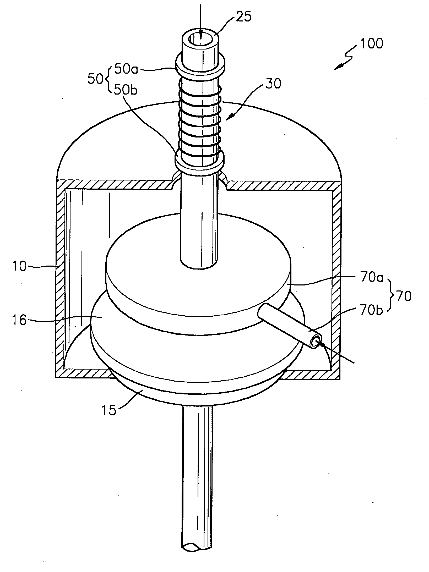
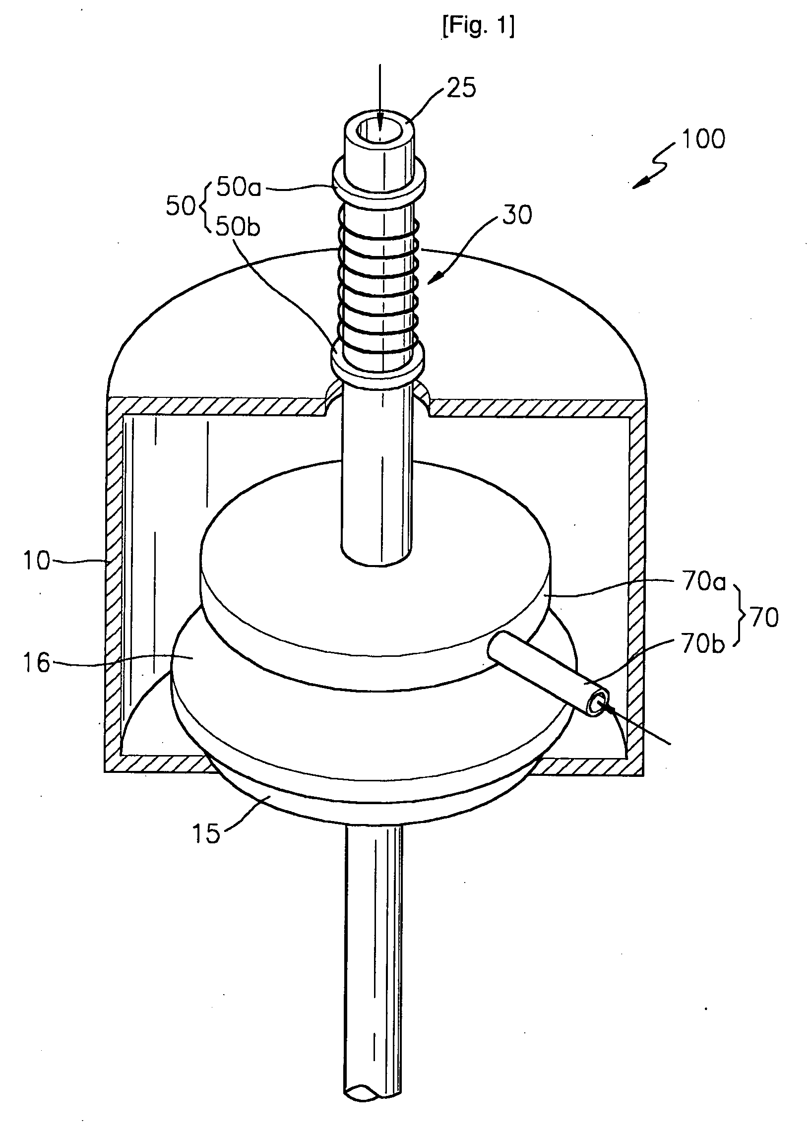
[0018]FIG. 1 is a schematic diagram of a remote plasma ALD apparatus 100 using a DC bias according to an embodiment of the present invention.

[0019]The remote plasma ALD apparatus 100 comprises an inner reaction chamber10 for forming a thin film, a remote plasma generating unit 30 for generating plasma, a DC bias unit 50 for controlling the remote plasma, and a source gas supply unit 70.

[0020]The inner reaction chamber 10 has an inner space in which a thin film is formed. A substrate supporting body 15 is arranged at one side in the inner space of the inner reaction chamber 10. A substrate 16 on which a thin film is to be formed is loaded onto the substrate supporting body 15. The substrate 16 may be composed of Si, and SiGe, Ge, Al2O3, GaAs or SiC.

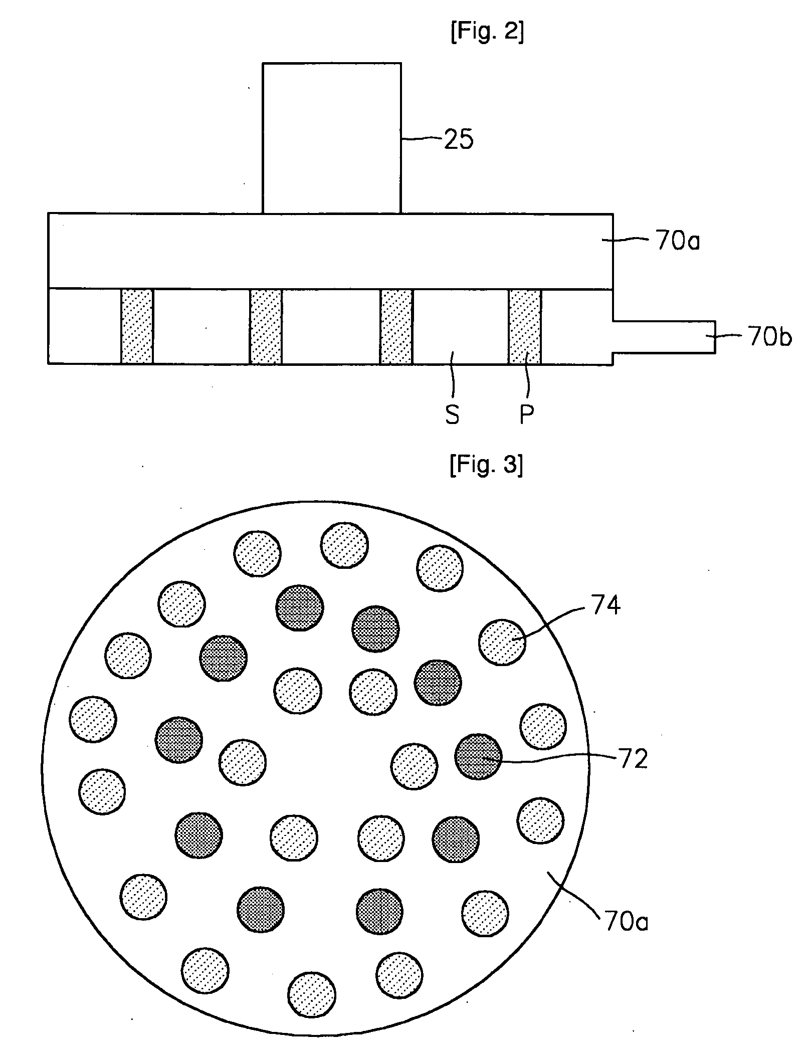
[0021]The source gas supply unit 70 supplies a source gas used to form the thin film into the inner reaction chamber 10. If the thin film to be grown on the substrate 16 is composed of a silicon compound such as silicon oxide, the correspo...


PUM

PropertyMeasurementUnit
frequencyaaaaaaaaaa
energyaaaaaaaaaa
controlling energyaaaaaaaaaa

Abstract

A conventional plasma applied ALD apparatus has a problem in that physical shock is directly imposed on a substrate and a thin film thereby damaging the thin film. Further, many reports have said that since an apparatus for controlling plasma energy is not arranged well, the thin film is not formed uniformly due to plasma nonuniformity. Therefore, there is provided a remote plasma atomic layer deposition apparatus using a DC bias comprising: a reaction chamber having an inner space; a substrate supporting body on which a substrate on which a thin film is to be formed is loaded arranged at one side of the inner space of the reaction chamber; a remote plasma generating unit arranged outside of the reaction chamber to supply a remote plasma into the inner space of the reaction chamber; a DC bias unit controlling energy of the remote plasma; and a source gas supply unit supplying a source gas for forming the thin film into the reaction chamber.

Description

TECHNICAL FIELD[0001]The present invention relates to a method and apparatus for forming a thin film, and more specifically, to an atomic layer deposition (ALD) apparatus and method capable of forming a thin film at an atomic level.BACKGROUND ART[0002]Thin films are used for various purposes such as a dielectric layer or an active layer of a semiconductor device, a transparent electrode of a liquid crystal display device, and an emission layer and a protective layer of an electroluminescent display device. However, with the development of technology, there is increasing need for a thin film having uniform thickness ranging from several nanometers to several tens of nanometers in an opto-electronic device and a display device, etc.[0003]Typically, the thin film is formed by using a physical deposition method such as sputtering or evaporation, a chemical deposition method such as chemical vapor deposition, and an ALD method etc. In the ALD method, a thin film is formed by decomposing ...

Claims


Application Information

Patent Timeline
Patent Type & Authority Applications(United States)
IPC IPC(8): B01J19/08C23C16/54
CPCC23C16/452C23C16/45525C23C16/45542C23C16/45544C23C16/45565H05H3/02C30B25/105H01J37/32082H01J37/32357H01J37/3244C23C16/45574
Inventor JEON, HYEONG-TAGKIM, UN-JUNGKIM, JU-YOUNKIM, JIN-WOO
Owner IUCF HYU (IND UNIV COOP FOUNDATION HANYANG UNIV)
Why Eureka
Try Eureka