Chip package process
a chip and package technology, applied in the field of semiconductor devices, can solve the problems of damage of the contact pad, and non-alignment between the chip and the substrate, and achieve the effect of reducing the warpage of the substra
- Summary
- Abstract
- Description
- Claims
- Application Information
AI Technical Summary
Benefits of technology
Problems solved by technology
Method used
Image

Examples
Embodiment Construction
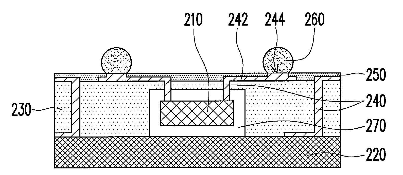
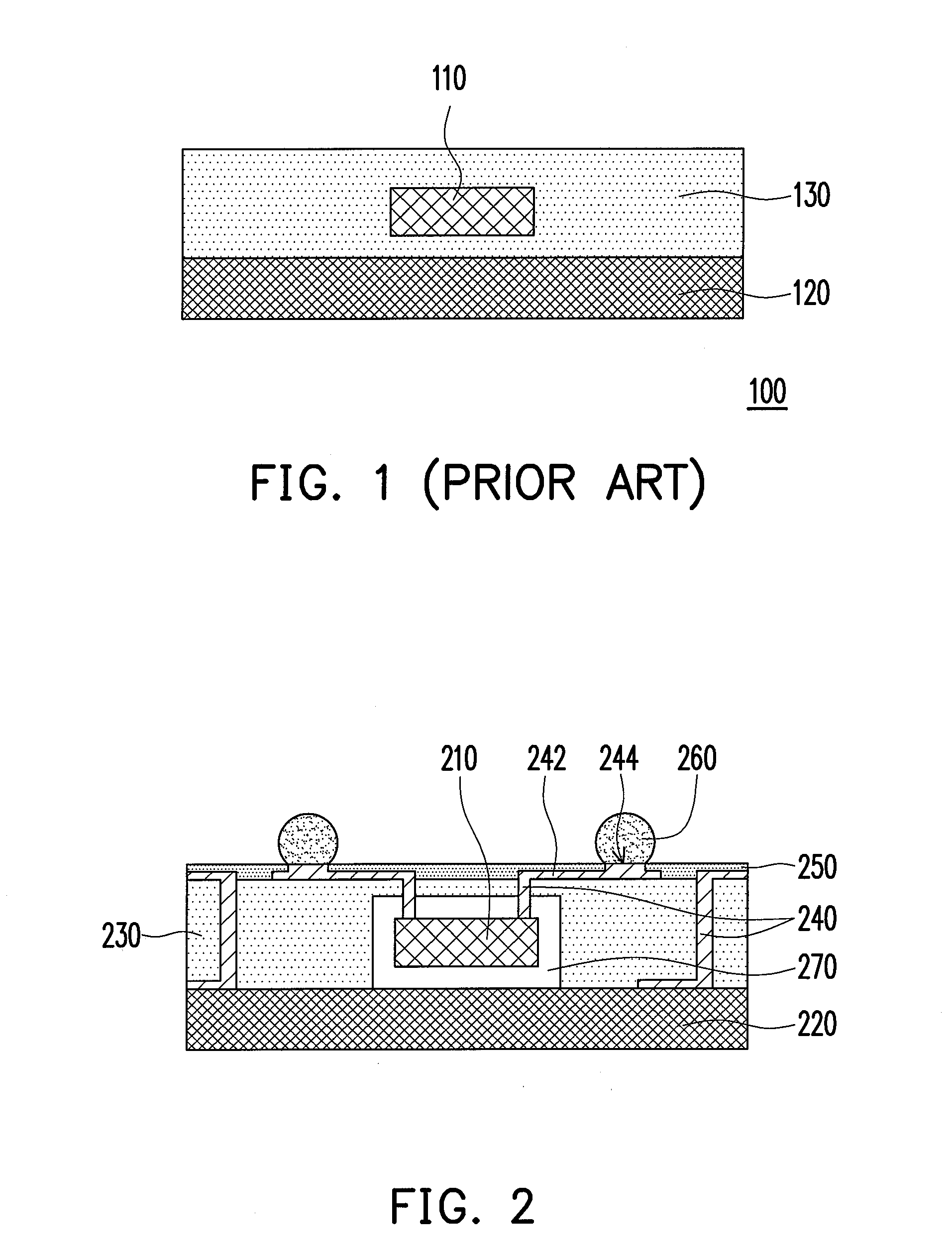
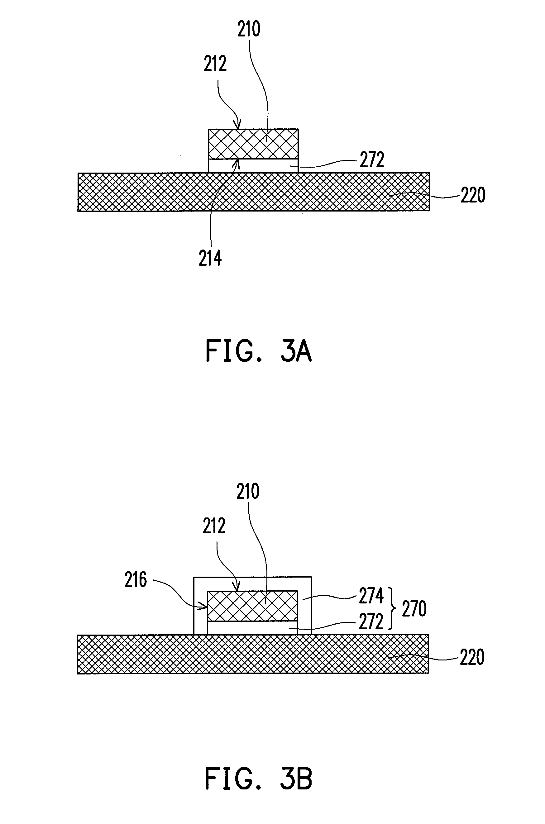
[0033]FIG. 2 is a schematic drawing of a chip package structure provided by an embodiment of the present invention. Referring to FIG. 2, to provide a chip 210 with a stress buffering effect, surrounding the chip 210 a buffering compound 270 is disposed and the chip 210 is disposed over the substrate 220 through the buffering compound 270. In addition, a dielectric material 230 covers the buffering compound 270 and the chip 210 and in the buffering compound 270 and the dielectric material 230 a plurality of interconnection traces 240 is formed.
[0034]Referring to FIG. 2 again, a part of the interconnection traces 240 are connected to subsurface circuits 242 on the surface of the dielectric material 230, while a passivation layer 250 is disposed on the dielectric material 230 for exposing a part of the subsurface circuit 242 and using the exposed portions as a plurality of contacts 244. Besides, on the contacts 244, solder balls 260 are disposed, so that the chip 210 can be connected t...
PUM
 Abstract
Description
Claims
Application Information
 - R&D
- Intellectual Property
- Life Sciences
- Materials
- Tech Scout
- Unparalleled Data Quality
- Higher Quality Content
- 60% Fewer Hallucinations
Browse by: Latest US Patents, China's latest patents, Technical Efficacy Thesaurus, Application Domain, Technology Topic, Popular Technical Reports.
© 2025 PatSnap. All rights reserved.Legal|Privacy policy|Modern Slavery Act Transparency Statement|Sitemap|About US| Contact US: help@patsnap.com