Nonvolatile memory element, nonvolatile memory apparatus, and method of manufacture thereof

a nonvolatile memory and memory element technology, applied in the direction of bulk negative resistance effect devices, electrical devices, semiconductor devices, etc., can solve the problems of crosstalk between contiguous cross points, deformation of electric characteristics as well as resistance varying characteristics, etc., to prevent damage to the sidewall of a variable resistance layer, the effect of suppressing crosstalk

Active Publication Date: 2009-01-15
PANASONIC SEMICON SOLUTIONS CO LTD
View PDF3 Cites 37 Cited by
  • Summary
  • Abstract
  • Description
  • Claims
  • Application Information

AI Technical Summary

Benefits of technology

[0027]In accordance with the nonvolatile memory elements and the nonvolatile memory apparatus of the present invention, the occurrence of c

Problems solved by technology

In this case, when etching away the resistance varying material in the region except for the interelectrode region between the upper electrode and the lower electrode, it is likely that the sidewalls of the variable resistance layer remaining in the interelectrode

Method used


Image

  • Nonvolatile memory element, nonvolatile memory apparatus, and method of manufacture thereof
  • Nonvolatile memory element, nonvolatile memory apparatus, and method of manufacture thereof
  • Nonvolatile memory element, nonvolatile memory apparatus, and method of manufacture thereof

Examples


first embodiment

Structure of Nonvolatile Memory Element

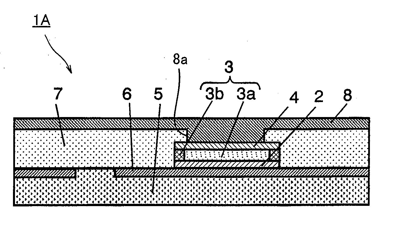
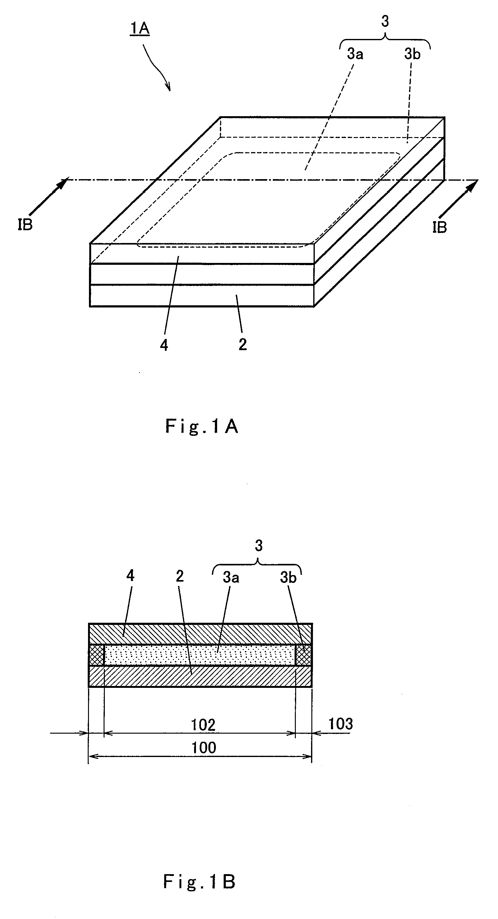
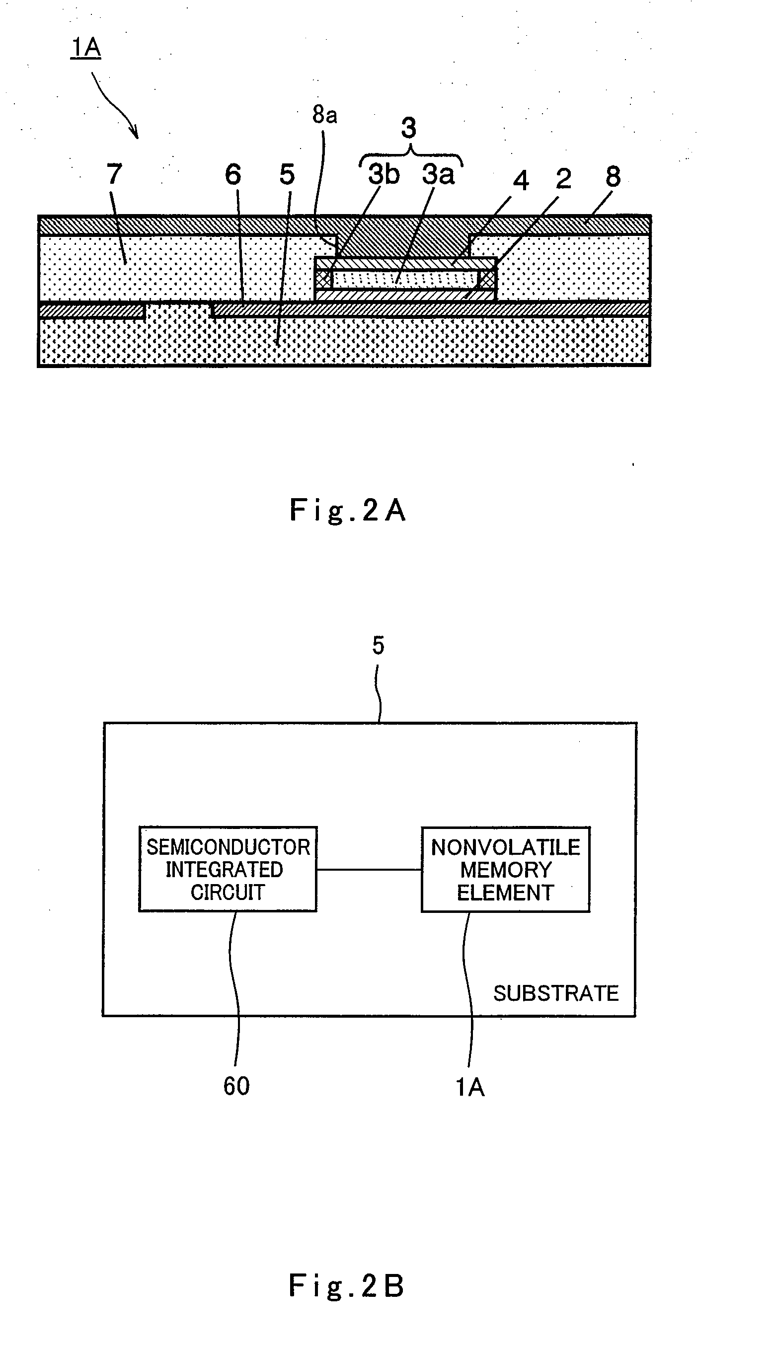
[0123]FIG. 1A is a perspective view illustrating schematically a structure of a principal part of a memory section in a nonvolatile memory element in accordance with a first embodiment of the present invention. FIG. 1B is a cross-sectional view depicting a cross section taken along line IB-IB of FIG. 1A. As shown in FIGS. 1A and 1B, a nonvolatile memory element 1A of the present invention includes a lower electrode layer 2 and an upper electrode layer 4 formed overlying the lower electrode layer 2. Formed between the lower electrode layer 2 and the upper electrode layer 4 is a metal oxide thin film layer 3.

[0124]The metal oxide thin film layer 3 is composed of a first region 3a and a second region 3b arranged so as to enclose the outer periphery of the first region 3a. In other words, the inner region of the metal oxide thin film layer 3 corresponds to the first region 3a and the outer peripheral region of the metal oxide thin film layer 3 corr...

second embodiment

[0166]A nonvolatile memory apparatus in accordance with a second embodiment is of a so-called cross point type in which an active layer is interposed at the cross point (cross point in three dimensions) of a word line and a bit line.

Structure of Nonvolatile Memory Apparatus

[0167]FIG. 8A is a perspective view illustrating schematically a structure of a principal part in the nonvolatile memory apparatus in accordance with the second embodiment of the present invention. FIG. 8B is a cross-sectional view depicting a cross section taken along line VIIIB-VIIIB of FIG. 8A. In addition, for the sake of convenience, the structural representation of the substrate, the interlayer dielectric layer and so on is omitted in part in FIGS. 8A and 8B.

[0168]As shown in FIGS. 8A and 8B, in the nonvolatile memory apparatus 10 of the present embodiment, a plurality of first electrode wires 11 are formed on a substrate (not shown). Each of the plurality of first electrode wires 11 is shaped like an elonga...

third embodiment

[0194]For the case of the nonvolatile memory apparatus of the second embodiment, the metal oxide thin film layers of the nonvolatile memory elements arrayed in a matrix are mutually physically separated from one another. On the other hand, in a nonvolatile memory apparatus of a third embodiment of the present invention, the metal oxide thin film layers of the nonvolatile memory elements are formed integrally with one another, as will be described hereinafter. That is, the metal oxide thin film layers of the adjacent nonvolatile memory elements in the second embodiment constitute an integral layer in the third embodiment.

Structure of Nonvolatile Memory Apparatus

[0195]FIG. 12A is a perspective view illustrating schematically a structure of a principal part of the nonvolatile memory apparatus in accordance with the third embodiment of the present invention. FIG. 12B is a cross-sectional view depicting a cross section taken along line XIIB-XIIB of FIG. 12A. Also note that for the sake o...


PUM


Abstract

A lower electrode layer 2, an upper electrode layer 4 formed above the lower electrode layer 2, and a metal oxide thin film layer 3 formed between the lower electrode layer 2 and the upper electrode layer 4 are provided. The metal oxide thin film layer 3 includes a first region 3a whose value of resistance increases or decreases by an electric pulse that is applied between the lower electrode layer 2 and the upper electrode layer 4 and a second region 3b arranged around the first region 3a and having a larger content of oxygen than the first region 3a, wherein the lower and upper electrode layers 2 and 4 and at least a part of the first region 3a are arranged so as to overlap as viewed from the direction of the thickness of the first region 3a.

Description

TECHNICAL FIELD[0001]The present invention relates to a nonvolatile memory element and a nonvolatile memory apparatus for storing data by the use of a material whose value of resistance varies reversibly by the application of an electric pulse and to a method of manufacture thereof.[0002]With the recent advance of digital technologies in the field of electronics devices, there are increasing demands for larger-capacity nonvolatile memory elements that are used to store data such as music data, image data, information data and so on. A memory element, which employs a material capable of varying in the value of resistance by the application of an electric pulse and of remaining in that state, has attracted attention as a measure to meet the demands.[0003]FIG. 21 is a principal part cross-sectional view illustrating the structure of a first conventional example (see, for example, Patent Document 1) of the aforesaid nonvolatile memory element. In this conventional nonvolatile memory ele...

Claims


Application Information

Patent Timeline
IPC IPC(8): H01L45/00
CPCH01L27/101H01L45/1658H01L45/1675H01L27/2472H01L27/2463H01L45/1233H01L45/146H01L27/2409H01L45/04H10B63/82H10B63/20H10B63/80H10N70/20H10N70/826H10N70/8833H10N70/046H10N70/063
Inventor KAWASHIMA, YOSHIOTAKAGI, TAKESHIMIKAWA, TAKUMIWEI, ZHIQIANG
Owner PANASONIC SEMICON SOLUTIONS CO LTD
Why Eureka
Try Eureka