Broadband transition from a via interconnection to a planar transmission line in a multilayer substrate

a multi-layer substrate and transmission line technology, applied in the direction of multi-port networks, cross-talk/noise/interference reduction, high-frequency circuit adaptations, etc., can solve the problem of large return loss, dramatically degrade the transmission of high-speed signals at the transceiver, and the characteristic impedance mismatching of the planar transmission line can be increased. problem, to achieve the effect of high electrical performance of the via structur

Active Publication Date: 2009-01-15
RENESAS ELECTRONICS CORP +1
View PDF2 Cites 31 Cited by
  • Summary
  • Abstract
  • Description
  • Claims
  • Application Information

AI Technical Summary

Benefits of technology

[0006]The cross-sectional form of the clearance hole in a via structure can be large enough compared with via pad dimensions and can take not only circular form but also various shapes (as for example, rectangular, square, elliptical and other complicated shapes) t

Problems solved by technology

Design of high-performance high-speed electrical circuits is one of the most important issues to implement interconnections based on multilayer substrate technologies.
As for an example, characteristic impedance mismatch can lead to large return losses that can dramatically degrade transferring high-speed signals at the transceiver.
However, such transition from the pad to the planar transmission line can give an increase of the characteristic impedance mismatching at higher frequencies due to the excess inductive reactance of a part of the transmission line disposed at the clearance hole area for which g

Method used


Image

  • Broadband transition from a via interconnection to a planar transmission line in a multilayer substrate
  • Broadband transition from a via interconnection to a planar transmission line in a multilayer substrate
  • Broadband transition from a via interconnection to a planar transmission line in a multilayer substrate

Examples


Embodiment Construction

[0063]The following description of the preferred embodiments directed to only several types of transitions from the via pad to the planar transmission line but it is well understood that this description should not be viewed as narrowing the claims which follows.

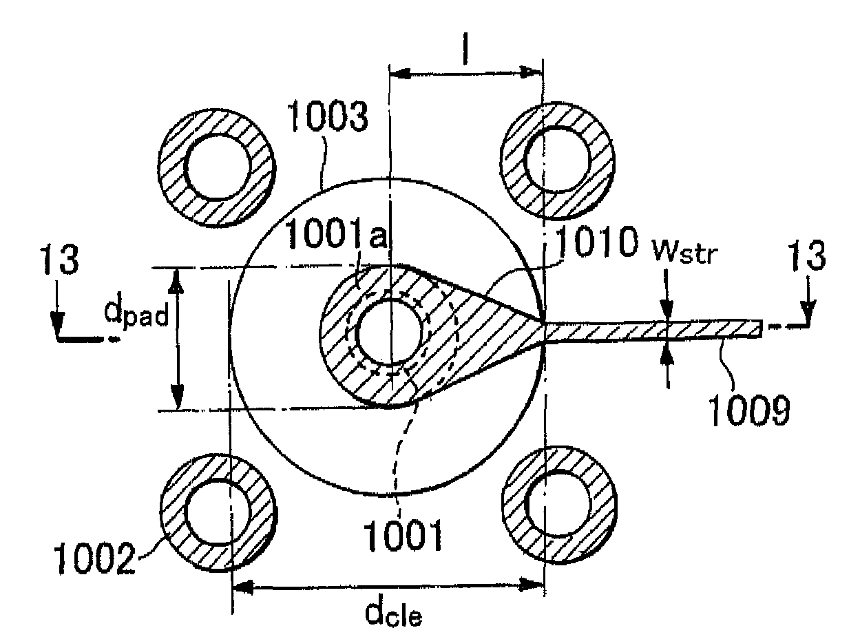
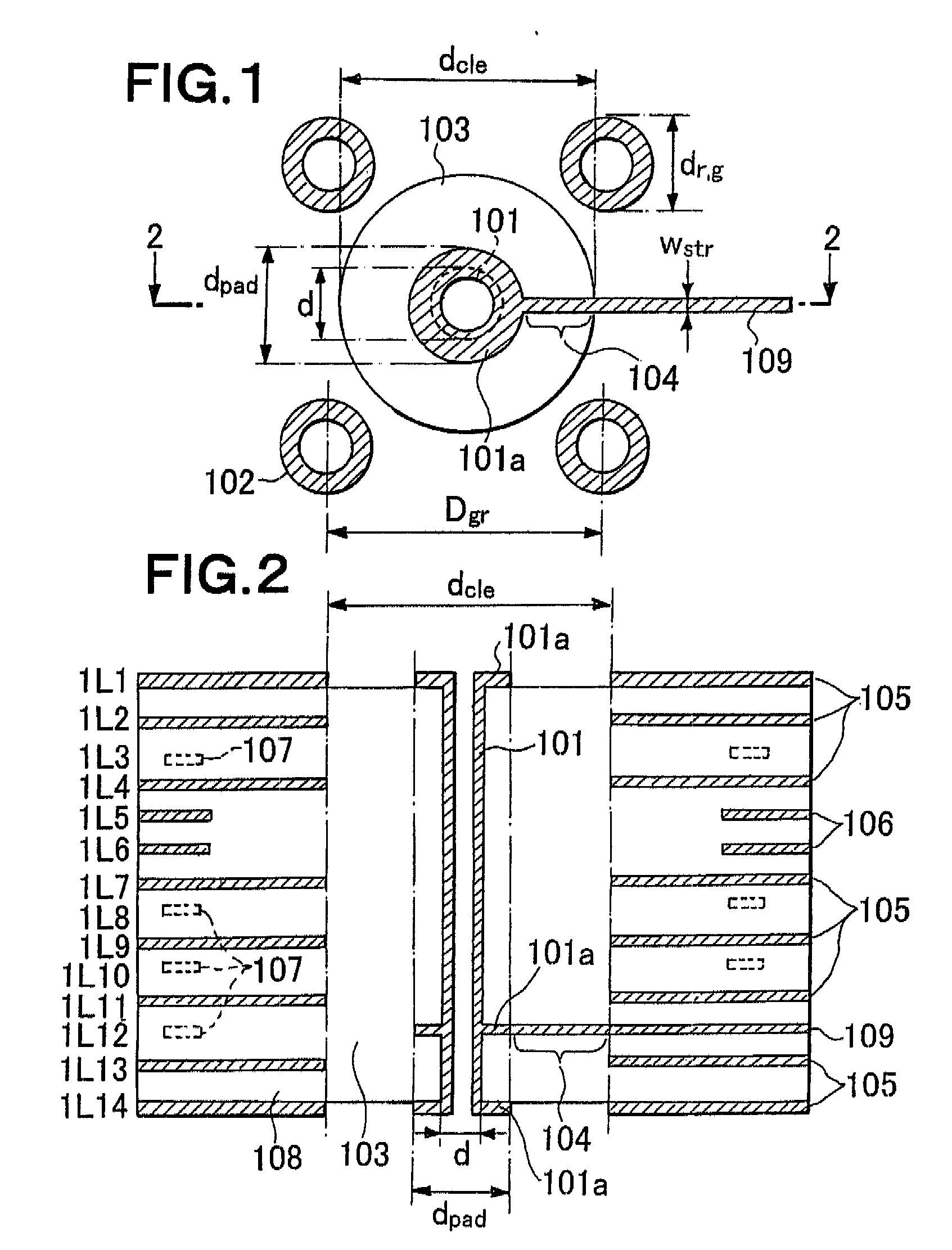
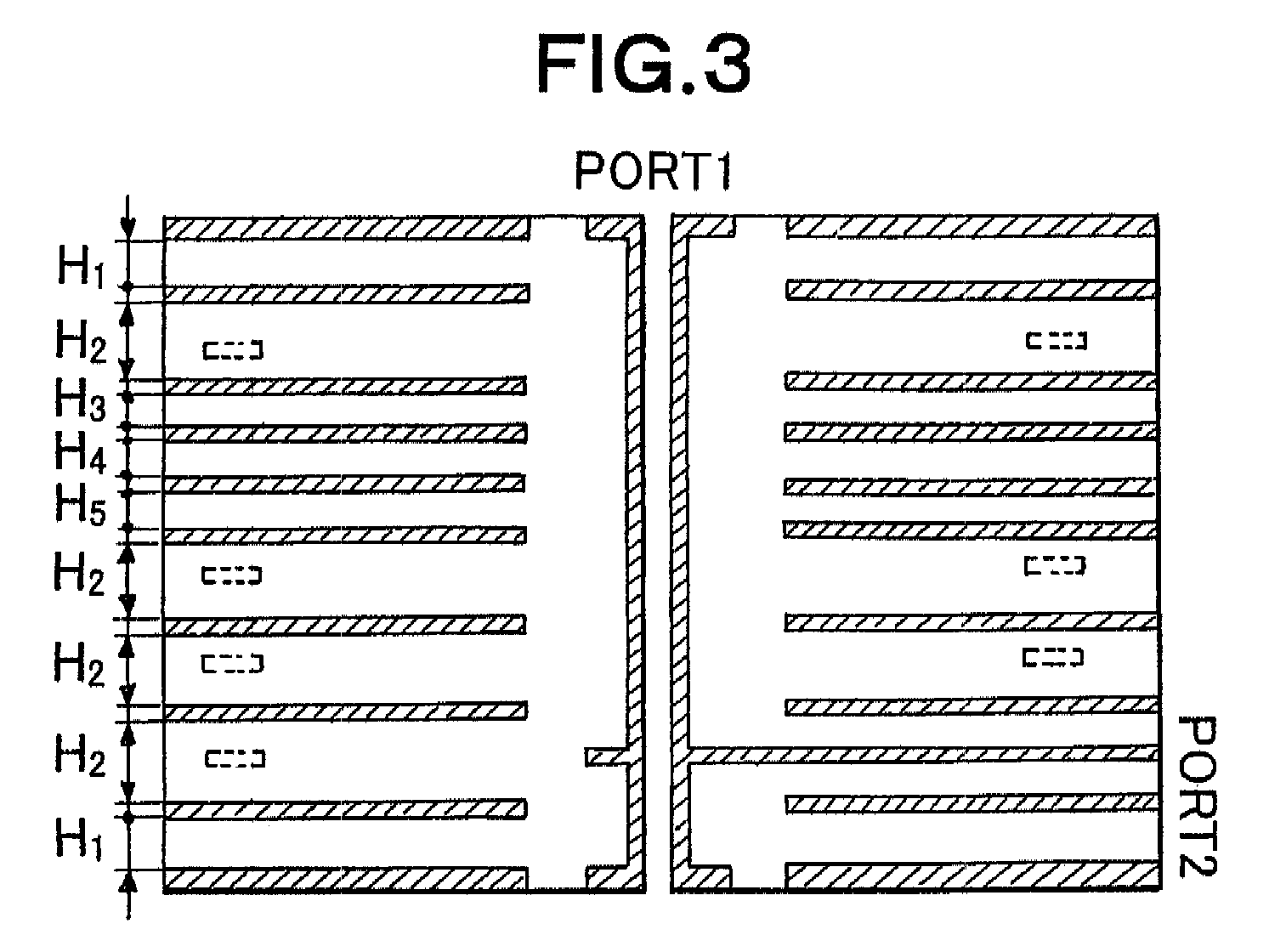
[0064]Referring to the drawings, a via structure in a 14-conductor-layer printed circuit board (PCB), which serve only as an example of via structure and multilayer PCB design, is shown in FIGS. 1 and 2. In these figures, the arrangement of planar conductor layers of the PCB separated by an isolating material 108 is as follows: Ground planes are 1L1, 1L2, 1L4, 1L7, 1L9, 1L11, 1L13 and 1L14 layers; Power supplying planes are 1L5 and 1L6 layers; and signal planes are 1L3, 1L8, 1L10, and 1L12 layers. The via structure consists of a signal via 101, four ground vias 102 which are connected to the ground plates 105 and clearance hole 103 which separates the signal via from the planar conductor layers. At the signal layer 1L12, a s...


PUM


Abstract

According to one embodiment, a broadband transition to joint a via structure and a planar transmission line in a multilayer substrate is formed as an intermediate connection between the signal via pad and the planar transmission line disposed at the same conductor layer. The transverse dimensions of the transition are equal to the via pad diameter at the one end and strip width at another end; The length of the transition can be equal to the characteristic dimensions of the clearance hole in the direction of the planar transmission line or defined as providing the minimal excess inductive reactance in time-domain according to numerical diagrams obtained by three-dimensional full-wave simulations.

Description

TECHNICAL FIELD[0001]This invention relates generally to multilayer substrate technologies and, as more specifically, to a broadband transition from a via pad to a planar transmission line disposed at the same conductor layer of a multilayer substrate.BACKGROUND ART[0002]Design of high-performance high-speed electrical circuits is one of the most important issues to implement interconnections based on multilayer substrate technologies. As for an example, characteristic impedance mismatch can lead to large return losses that can dramatically degrade transferring high-speed signals at the transceiver. Multilayer substrates, which are cost-effective technologies, include planar conductive layers and vertical transitions connecting planar transmission line circuits disposed at different conductor layers. Vertical transitions in the multilayer substrate are usually realized by means of via structures.[0003]To join a via and a planar transmission line forming an interconnect circuit in a ...

Claims


Application Information

Patent Timeline
IPC IPC(8): H03H7/38
CPCH05K1/0219H05K1/0222H05K1/0245H05K1/0251H05K2201/09727H05K3/429H05K2201/09381H05K2201/09636H05K2201/09718H05K1/116
Inventor KUSHTA, TARASNARITA, KAORUKANEKO, TOMOYUKIOGOU, SHIN-ICHI
Owner RENESAS ELECTRONICS CORP
Why Eureka
Try Eureka