Method and program for designing semiconductor integrated circuit

a technology of integrated circuits and integrated circuits, applied in the direction of program control, cad circuit design, instruments, etc., can solve the problems of not being able to module the spice model parameter of pmos transistors pb>1, not being able to consider the dependence of peripheral patterns in spice simulation, and preventing the increase of design/verification ta

Inactive Publication Date: 2009-01-22
RENESAS ELECTRONICS CORP
View PDF10 Cites 326 Cited by
  • Summary
  • Abstract
  • Description
  • Claims
  • Application Information

AI Technical Summary

Benefits of technology

[0033]Therefore, the accuracy of the delay verification is improved. Consequently, yield and reliability of the semiconductor integrated circuit to be manufactured are also improved. Moreover, it is not necessary to repeat the SPICE simulation at the circuit design / verification stage. Therefore, increase in the design / verification TAT can be prevented.
[0034]Furthermore, the margin such as shown in FIG. 4 is not added to the delay value of each cell. Although a center value of the calculated cell delay value may vary from the normal one, the variability range is the same as the normal one. As a result, the number of repetition times of the layout design and delay verification is prevented from being increased. Therefore, the increase in the design / verification TAT can be prevented. Moreover, it is not necessary to increase driving capability of transistors and / or to additionally insert redundant cells. Therefore, the increase in the chip area and power consumption can be prevented.
[0037]According to the present invention, it is possible to prevent the increase in the design / verification TAT for the semiconductor integrated circuit, while considering the peripheral pattern dependence of the transistor characteristics sufficiently.

Problems solved by technology

Due to the OPE, a resist pattern may not be formed as intended, which causes deviations of interconnection width and gate size from the design values.
Therefore, it is not possible to module the SPICE model parameter of the PMOS transistor P1 prior to the SPICE simulation.
However, with regard to the outermost transistor placed near the cell boundary, it is not possible to consider the peripheral pattern dependence in the SPICE simulation since the peripheral layout pattern is unknown.
Consequently, it cannot be said that the accuracy of the delay verification (STA) is sufficient.
This contributes to reduction of yield and reliability of the semiconductor integrated circuit to be manufactured.
Furthermore, the first method is disadvantageous in that the corner condition of the cell delay value becomes stricter as compared with that in the method shown in FIG. 2. FIG. 4 schematically shows the corner condition (corner delay value) provided by the cell delay library.
In other words, it is necessary to repeat the layout design and delay verification until the design circuit operates in the corner condition.
This leads to increase in a chip area and power consumption.

Method used


Image

  • Method and program for designing semiconductor integrated circuit
  • Method and program for designing semiconductor integrated circuit
  • Method and program for designing semiconductor integrated circuit

Examples


first example

4-1. FIRST EXAMPLE

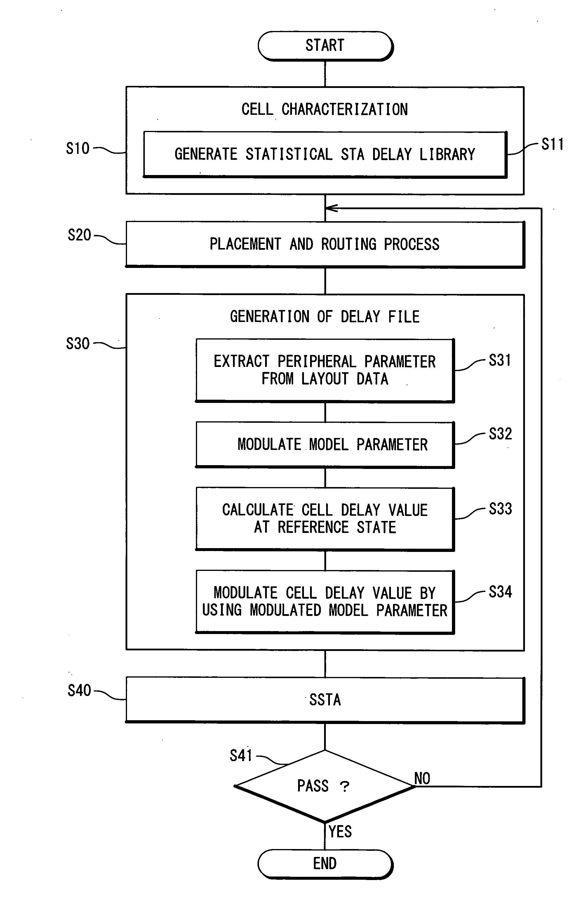
[0100]FIG. 10 is a block diagram showing a first example of a method of generating the delay file SDF. The pattern dependence consideration tool 10 reads the pre-modulation cell netlist D11 of the target cell and the layout data LAY generated in the foregoing Step S20. Then, the pattern dependence consideration tool 10 modulates the pre-modulation cell netlist D11 based on the layout data LAY.

[0101]More specifically, the pattern dependence consideration tool 10 extracts the peripheral parameters (gate pitch and STI width) associated with the target transistor included in the target cell, from the layout data LAY (Step S31). In particular, the pattern dependence consideration tool 10 extracts the peripheral parameters (PGP_L, PDS_L, PGP_R, PDS_R, NGP_L, NDS_L, NGP_R and NDS_R) associated with the outermost transistors (e.g. P1, P3, N1 and N4 in FIG. 5) placed at the outermost in the target cell.

[0102]Subsequently, the pattern dependence consideration tool 10 modulat...

second example

4-2. SECOND EXAMPLE

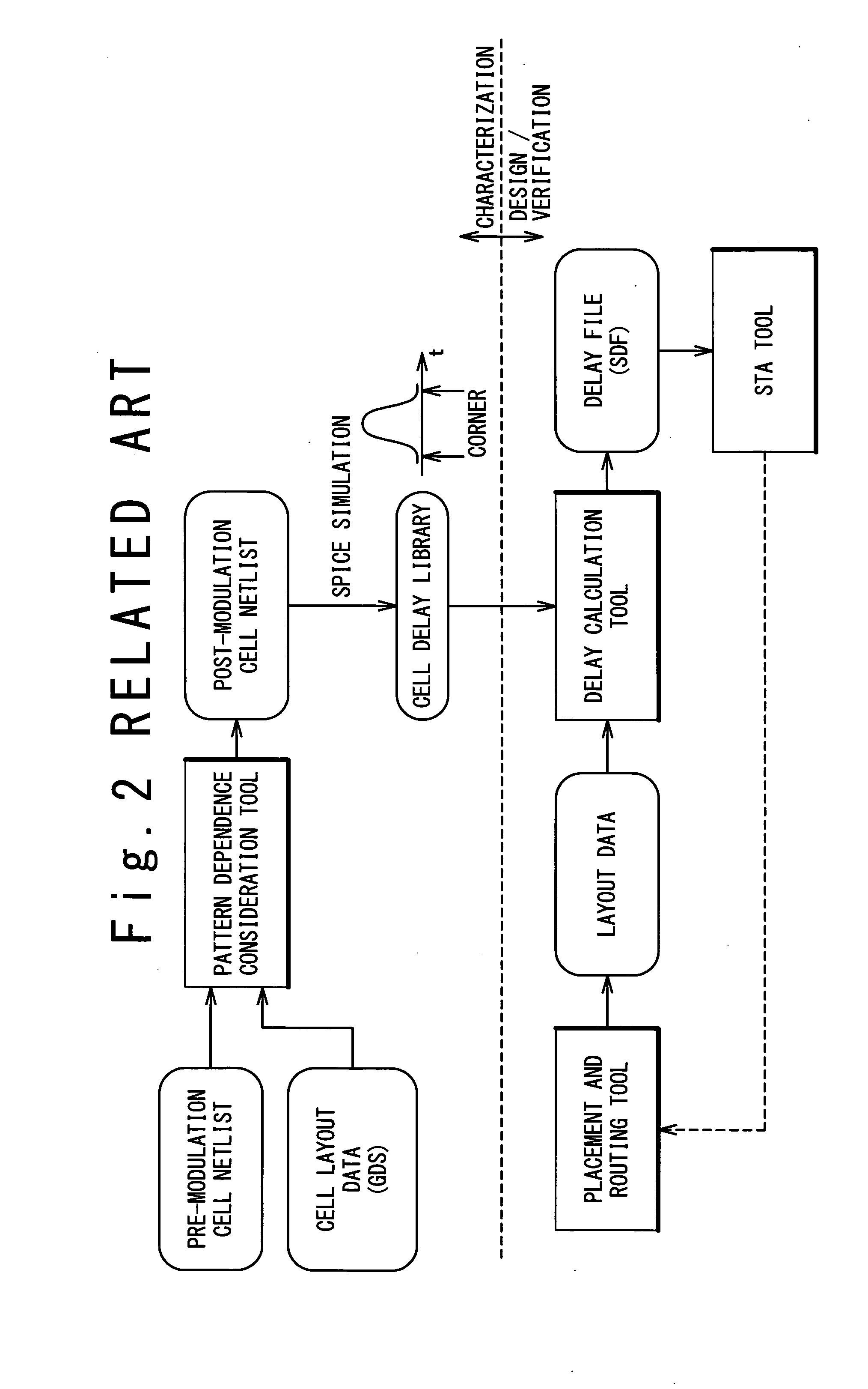
[0105]FIG. 11 is a block diagram showing a second example of a method of generating the delay file SDF. In the present example, the delay calculation tool 30 includes a conventional delay calculation tool 30-0 and a variation calculation tool 31. The delay calculation tool 30-0 generates a delay file SDF-0 as usual based on the layout data LAY and the statistical STA delay library LIB. That is, the delay calculation tool 30-0 generates the delay file SDF-0 without calculating the delay variation Δt. The delay file SDF-0 indicates the reference delay value t of each cell and the path delay values.

[0106]The variation calculation tool 31 calculates the above-mentioned delay variation Δt based on the statistical STA delay library LIB and the post-modulation cell netlist D30. Then, the variation calculation tool 31 reads the delay file SDF-0 and modifies the delay file SDF-0 by using the delay variation Δt. In other words, the variation calculation tool 31 reflects the...

third example

4-3. THIRD EXAMPLE

[0107]In the third example, the model parameter modulated by the pattern dependence consideration tool 10 does not match the model parameter treated by the statistical STA delay library LIB. In this case, it is necessary to convert the modulation amount of the model parameter output from the pattern dependence consideration tool 10 into a modulation amount of an appropriate model parameter.

[0108]For example, let us consider a case where variations of only gate length L and gate width W among the SPICE model parameters are considered in the statistical STA delay library LIB. In this case, the delay function expresses the cell delay value as a function of a gate length variation ΔL and a gate width variation ΔW (t=f (ΔL, ΔW)). Meanwhile, the modulation target parameters in the pattern dependence consideration tool 10 are mobility μ0 and threshold voltage VT0 among the SPICE model parameters. The modulation amounts of the model parameters μ0 and VT0 are Δμ0 and ΔVT0, ...


PUM


Abstract

A design method for an LSI includes: generating a delay library for use in a statistical STA, wherein the delay library provides a delay function that expresses a cell delay value as a function of model parameters of a transistor; generating a layout data; and calculating a delay value of a target cell based on the delay library and the layout data. The calculating includes: referring to the layout data to extract a parameter specifying a layout pattern around a target transistor; modulating model parameters of the target transistor such that the characteristics corresponding to the extracted parameter is obtained in a circuit simulation; calculating, by using the delay function, a reference delay value of the target cell; and calculating, by using the delay function and the modulation amount of the model parameter, a delay variation from the reference delay value depending on the modulation amount.

Description

INCORPORATION BY REFERENCE[0001]This application is based upon and claims the benefit of priority from Japanese patent application No. 2007-186255, filed on Jul. 17, 2007, the disclosure of which is incorporated herein in its entirely by reference.BACKGROUND OF THE INVENTION[0002]1. Field of the Invention[0003]The present invention relates to a design technique for a semiconductor integrated circuit. In particular, the present invention relates to a design technique in which layout around an element is considered.[0004]2. Description of Related Art[0005]Characteristics of a transistor depend on “device parameters” such as gate length L, gate width W, mobility μ, threshold voltage Vt and the like. When the transistor is actually manufactured, those device parameters are likely to vary from design values. The variations of the device parameters from the design values lead to variations of the transistor characteristics from expected values. It is therefore important to sufficiently co...

Claims


Application Information

Patent Timeline
Patent Type & Authority Applications(United States)
IPC IPC(8): G06F17/50
CPCG06F17/5036G06F2217/84G06F17/5068G06F30/367G06F30/39G06F2119/12
Inventor YAMADA, KENTA
Owner RENESAS ELECTRONICS CORP
Why Eureka
Try Eureka