Method of designing semiconductor integrated circuit and mask data generation program

a technology of integrated circuits and mask data, applied in the direction of cad circuit design, originals for photomechanical treatment, instruments, etc., can solve the problems of not being able to module the spice model parameter of pmos transistor pb>1, not being able to consider the dependence of peripheral pattern in spice simulation, and preventing the increase of design/verification tat

Inactive Publication Date: 2011-11-08
RENESAS ELECTRONICS CORP
View PDF19 Cites 8 Cited by
  • Summary
  • Abstract
  • Description
  • Claims
  • Application Information

AI Technical Summary

Benefits of technology

[0034]According to the present invention, as described above, the peripheral pattern dependence of the transistor characteristics is fully considered. Thus, yield and reliability of the semiconductor integrated circuit to be manufactured are improved. Moreover, increase in the characterization TAT and the design / verification TAT can be prevented, because the peripheral pattern dependence is considered at the mask data generation stage.
[0035]Furthermore, it is not necessary to add the margin such as shown in FIG. 4, since the peripheral pattern dependence needs not be considered at the cell characterization stage. As a result, the number of repetition times of the layout design and delay verification is prevented from being increased. Therefore, the increase in the design / verification TAT can be prevented. Moreover, it is not necessary to increase driving capability of transistors and / or to additionally insert redundant cells. Therefore, the increase in the chip area and power consumption can be prevented.
[0037]According to the present invention, it is possible to prevent the increase in the design / verification TAT for the semiconductor integrated circuit, while considering the peripheral pattern dependence of the transistor characteristics sufficiently.

Problems solved by technology

Due to the OPE, a resist pattern may not be formed as intended, which causes deviations of interconnection width and gate size from the design values.
Therefore, it is not possible to module the SPICE model parameter of the PMOS transistor P1 prior to the SPICE simulation.
However, with regard to the outermost transistor placed near the cell boundary, it is not possible to consider the peripheral pattern dependence in the SPICE simulation since the peripheral layout pattern is unknown.
Consequently, it cannot be said that the accuracy of the delay verification (STA) is sufficient.
This contributes to reduction of yield and reliability of the semiconductor integrated circuit to be manufactured.
Furthermore, the first method is disadvantageous in that the corner condition of the cell delay value becomes stricter as compared with that in the method shown in FIG. 2. FIG. 4 schematically shows the corner condition (corner delay value) provided by the cell delay library.
In other words, it is necessary to repeat the layout design and delay verification until the design circuit operates in the corner condition.
This leads to increase in a chip area and power consumption.

Method used


Image

  • Method of designing semiconductor integrated circuit and mask data generation program
  • Method of designing semiconductor integrated circuit and mask data generation program
  • Method of designing semiconductor integrated circuit and mask data generation program

Examples


modification example

[0097]3. Modification Example

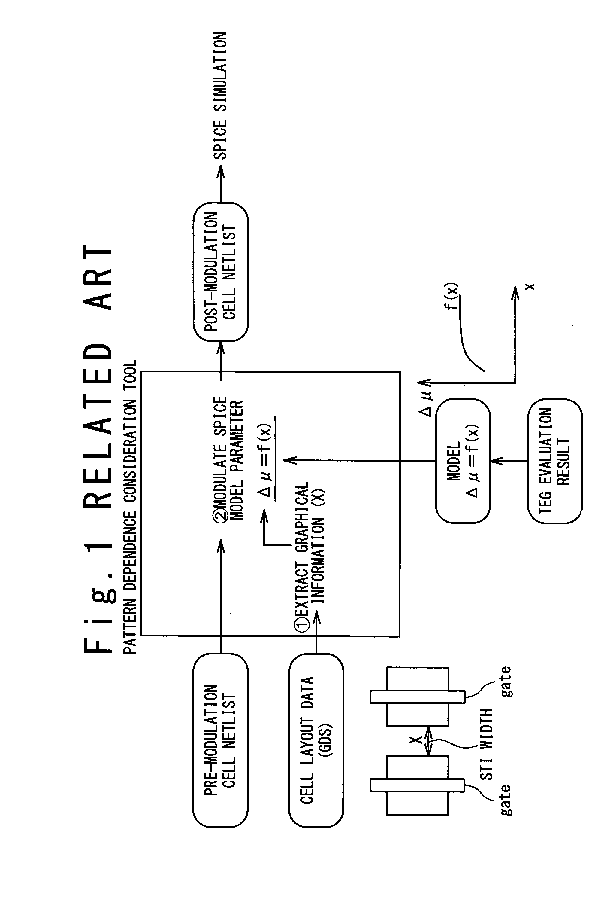
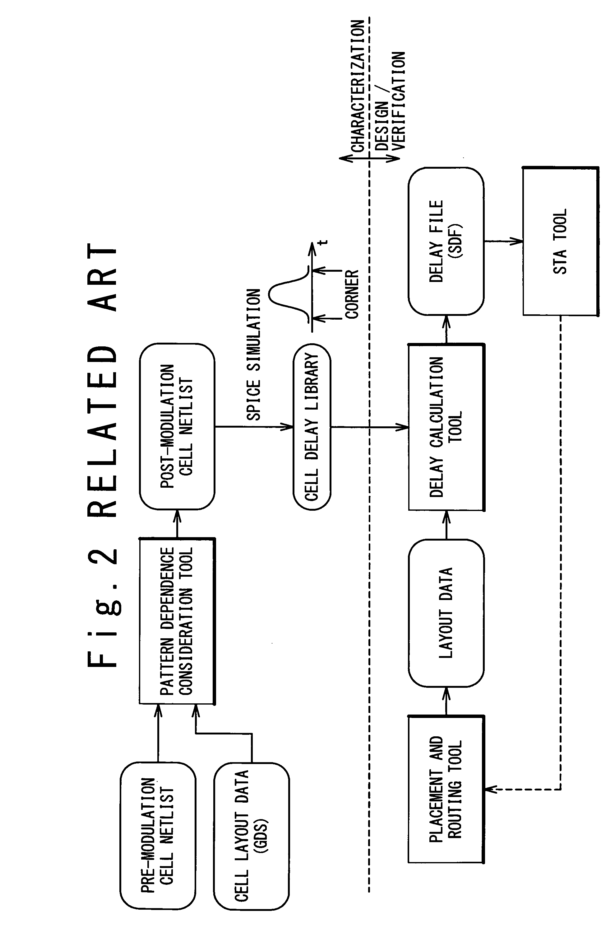
[0098]A method of the LW modulation is not limited to the above-described one. For example, the pattern dependence consideration tool explained in FIG. 1 can be utilized in calculating the LW modulation amounts (ΔL, ΔW). FIG. 11 is a block diagram for explaining a modification example of a method of calculating the LW modulation amounts. In the modification example, a pattern dependence consideration tool 50 and a parameter conversion tool 60 are used for calculating the LW modulation amounts.

[0099]First, the pattern dependence consideration tool 50 modulates SPICE model parameters based on the chip-level layout data LAY. More specifically, the pattern dependence consideration tool 50 reads a pre-modulation cell netlist CNET and the layout data LAY, and extracts the peripheral parameters (X1 to X4, Y1 to Y4, Z1 to Z2) of each transistor from the layout data LAY. Subsequently, the pattern dependence consideration tool 50 modulates SPICE model parameters i...


PUM

PropertyMeasurementUnit
widthaaaaaaaaaa
gate lengthaaaaaaaaaa
lengthaaaaaaaaaa

Abstract

A method of designing a semiconductor integrated circuit includes: generating a layout data indicating a layout; and generating a mask data based on the layout data. The generating the mask data includes: referring to the layout data to extract a parameter that specifies a layout pattern around a target transistor included in the semiconductor integrated circuit, wherein the parameter includes at least a width of a device isolation structure around the target transistor; correcting a gate length and a gate width of the target transistor to offset a variation of a characteristic of the target transistor from a design value, the variation depending on the extracted parameter; and generating the mask data from the layout data in which the gate length and the gate width are corrected.

Description

INCORPORATION BY REFERENCE[0001]This application is based upon and claims the benefit of priority from Japanese patent application No. 2007-186191, filed on Jul. 17, 2007, the disclosure of which is incorporated herein in its entirely by reference.BACKGROUND OF THE INVENTION[0002]1. Field of the Invention[0003]The present invention relates to a design technique for a semiconductor integrated circuit. In particular, the present invention relates to a design technique in which layout around an element is considered.[0004]2. Description of Related Art[0005]Characteristics of a transistor depend on “device parameters” such as gate length L, gate width W, mobility μ, threshold voltage Vt and the like. When the transistor is actually manufactured, those device parameters are likely to vary from design values. The variations of the device parameters from the design values lead to variations of the transistor characteristics from expected values. It is therefore important to sufficiently co...

Claims


Application Information

Patent Timeline
Patent Type & Authority Patents(United States)
IPC IPC(8): G06F17/50G06F11/22G03F1/36G03F1/68G03F1/70H01L21/82
CPCG06F17/5068G06F30/39
Inventor YAMADA, KENTA
Owner RENESAS ELECTRONICS CORP
Why Eureka
Try Eureka