Semiconductor Device and Method for Manufacturing the Same

a technology of semiconductor devices and heat sinks, which is applied in the direction of semiconductor devices, semiconductor/solid-state device details, electrical apparatus, etc., can solve the problems of prolonging the operation life of devices, and achieve the effect of preventing the optical and electrical properties of semiconductor devices from being damaged and greatly enhancing the heat dissipation ability of semiconductor devices

Inactive Publication Date: 2009-01-29
CHEN KUAN CHUN
View PDF6 Cites 10 Cited by
  • Summary
  • Abstract
  • Description
  • Claims
  • Application Information

AI Technical Summary

Benefits of technology

[0007]Therefore, one aspect of the present invention is to provide a semiconductor device, in which a semiconductor chip can be closely connected to a heat sink by a high electricity conducting thin film and a high heat conducting thick film directly without using glue materials. As a result, the heat-dissipating ability of semiconductor device can be greatly enhanced, and a high temperature process for fixing the semiconductor chip is eliminated to prevent the optical and electrical properties of the semiconductor device from being damaged.

Problems solved by technology

In addition, a large amount of heat generated by the semiconductor device with superior heat-dissipating ability operating at a high operation speed can be rapidly conducted and dissipated, so that it can prevent the semiconductor device from being burned out by a high temperature, thereby greatly prolonging the operation life of the device.

Method used


Image

  • Semiconductor Device and Method for Manufacturing the Same
  • Semiconductor Device and Method for Manufacturing the Same
  • Semiconductor Device and Method for Manufacturing the Same

Examples


Embodiment Construction

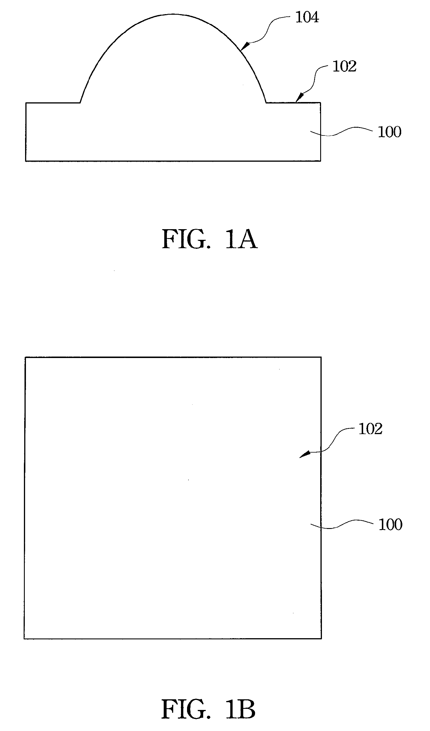
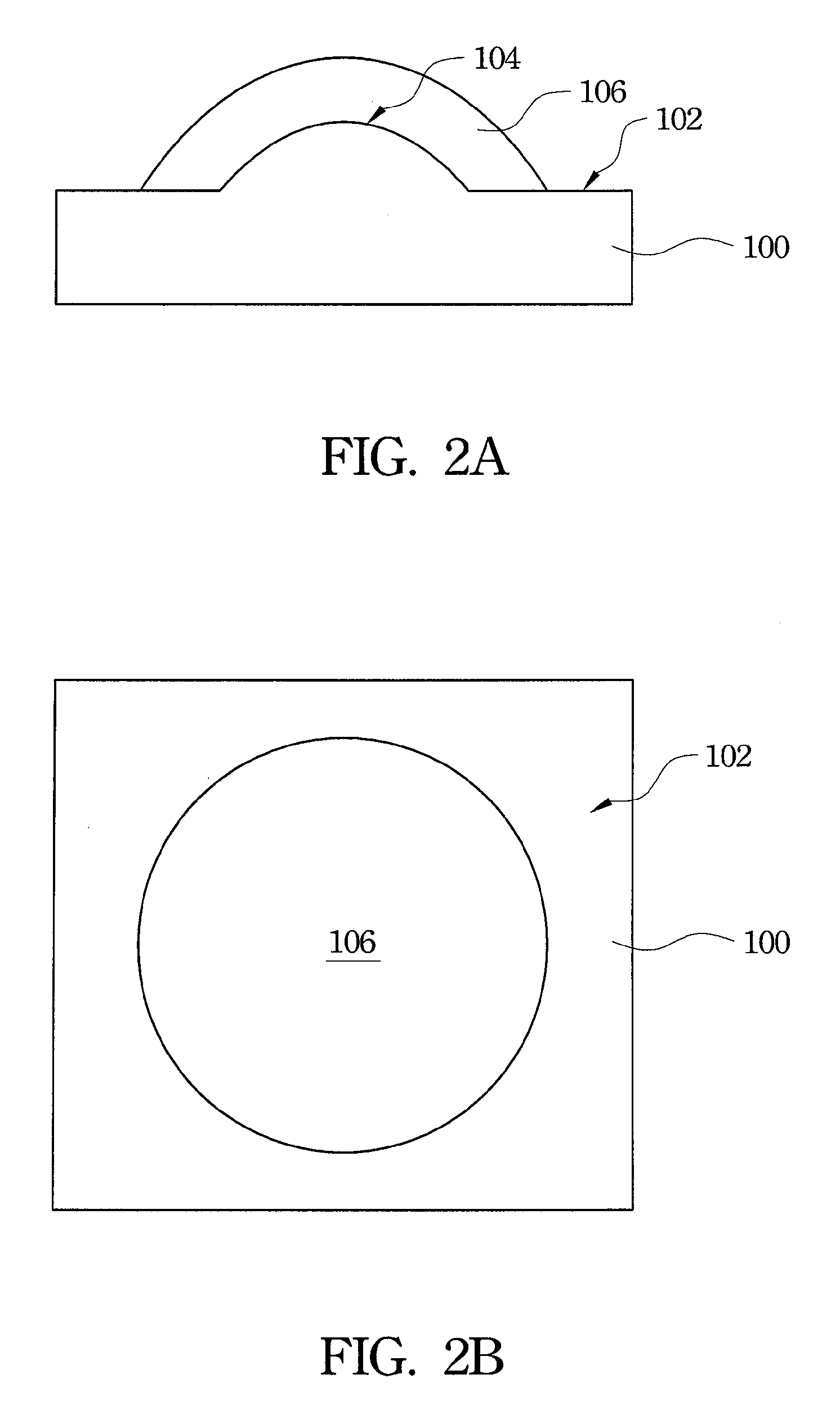
[0020]The present invention discloses a semiconductor device and a method for manufacturing the same. In order to make the illustration of the present invention more explicit, the following description is stated with reference to FIG. 1A through to FIG. 10B.

[0021]FIG. 1 through FIG. 10B are schematic flow diagrams showing the process for manufacturing a semiconductor device in accordance with a preferred embodiment of the present invention, wherein the schematic flow diagrams includes cross-sectional views and the corresponding top views. In an exemplary embodiment, when a semiconductor device is manufactured, a mold 100 is provided, such as shown in shown in FIG. 1A and FIG. 1B, wherein FIG. 1A is the cross-sectional view and FIG. 1B is the corresponding top view. In the present invention, the mold may include a flat surface, so the mold may be a flat substrate; or the shape of the mold may be designed according to the needs of a product to make the surface of the mold include a th...


PUM


Abstract

A semiconductor device and a method for manufacturing the same are described. The semiconductor device comprises: a heat sink having at least one opening passing through the heat sink; at least one semiconductor chip disposed in the opening, wherein the semiconductor chip includes a first side and a second side on opposite sides; an electricity conducting thin film filling in a first depth portion of the opening, wherein the second side of the semiconductor chip is embedded in the electricity conducting thin film; a heat conducting thick film filling in a second depth portion of the opening, wherein the electricity conducting thin film is directly connected with the heat conducting thick film; at least one wire electrically connecting the semiconductor chip and an external circuit; and an encapsulant covering a portion of the heat sink, the semiconductor chip, the wire and an exposed portion of the electricity conducting thin film.

Description

RELATED APPLICATIONS[0001]This application claims priority to Taiwan Application Serial Number 96126709, filed Jul. 20, 2007, which is herein incorporated by reference.FIELD OF THE INVENTION[0002]The present invention relates to a semiconductor device and a method for manufacturing the same, and more particularly, to a semiconductor device with a heat sink and a method for manufacturing the same.BACKGROUND OF THE INVENTION[0003]Currently, packaging techniques for semiconductor devices, such as transistors, integrated circuits, or opto-electrical devices including light-emitting diodes (LEDs) and laser diodes (LDs), include using glue or silver solder paste to connect semiconductor chips and frames or sub-mounts while flip-chip techniques are performed by using metal bumps to connect semiconductor chips and package substrates or frames. The glue or silver solder paste is usually mixed with polymer materials to provide viscosity.[0004]The glue or solder paste is usually mixed with pol...

Claims


Application Information

Patent Timeline
Patent Type & Authority Applications(United States)
IPC IPC(8): H01L23/36H01L21/58
CPCH01L23/36H01L24/48H01L33/642H01L33/647H01L2224/32188H01L2224/48091H01L2924/01078H01L2924/1305H01L2924/14H01L2924/00014H01L2924/00H01L2924/12041H01L2224/45099H01L2224/45015H01L2924/207
Inventor CHEN, KUAN-CHUN
Owner CHEN KUAN CHUN
Why Eureka
Try Eureka