Color filter plate and thin film transistor plate for liquid crystal display, and methods for fabricating the plates

a technology of liquid crystal display and color filter plate, which is applied in the direction of optical filter, optics, instruments, etc., can solve problems such as deteriorating picture quality, and achieve the effect of improving picture quality and preventing miss-orientation

Inactive Publication Date: 2009-01-29
SAMSUNG DISPLAY CO LTD
View PDF11 Cites 7 Cited by
  • Summary
  • Abstract
  • Description
  • Claims
  • Application Information

AI Technical Summary

Benefits of technology

[0007]It is an object of the present invention to provide a liquid crystal display which exhibits improved picture quality while preventing miss-orientation of liquid crystal molecules and leakage of light.

Problems solved by technology

However, in this case, the periphery of the color filter may involve a stepped difference so large as to change the molecular orientation of the liquid crystal while causing disclination.
Furthermore, the periphery of the color filter is liable to be under-cut while causing leakage of light at the black display state, and deteriorating the picture quality.

Method used


Image

  • Color filter plate and thin film transistor plate for liquid crystal display, and methods for fabricating the plates
  • Color filter plate and thin film transistor plate for liquid crystal display, and methods for fabricating the plates
  • Color filter plate and thin film transistor plate for liquid crystal display, and methods for fabricating the plates

Examples


Embodiment Construction

[0034]Preferred embodiments of this invention will be explained with reference to the accompanying drawings.

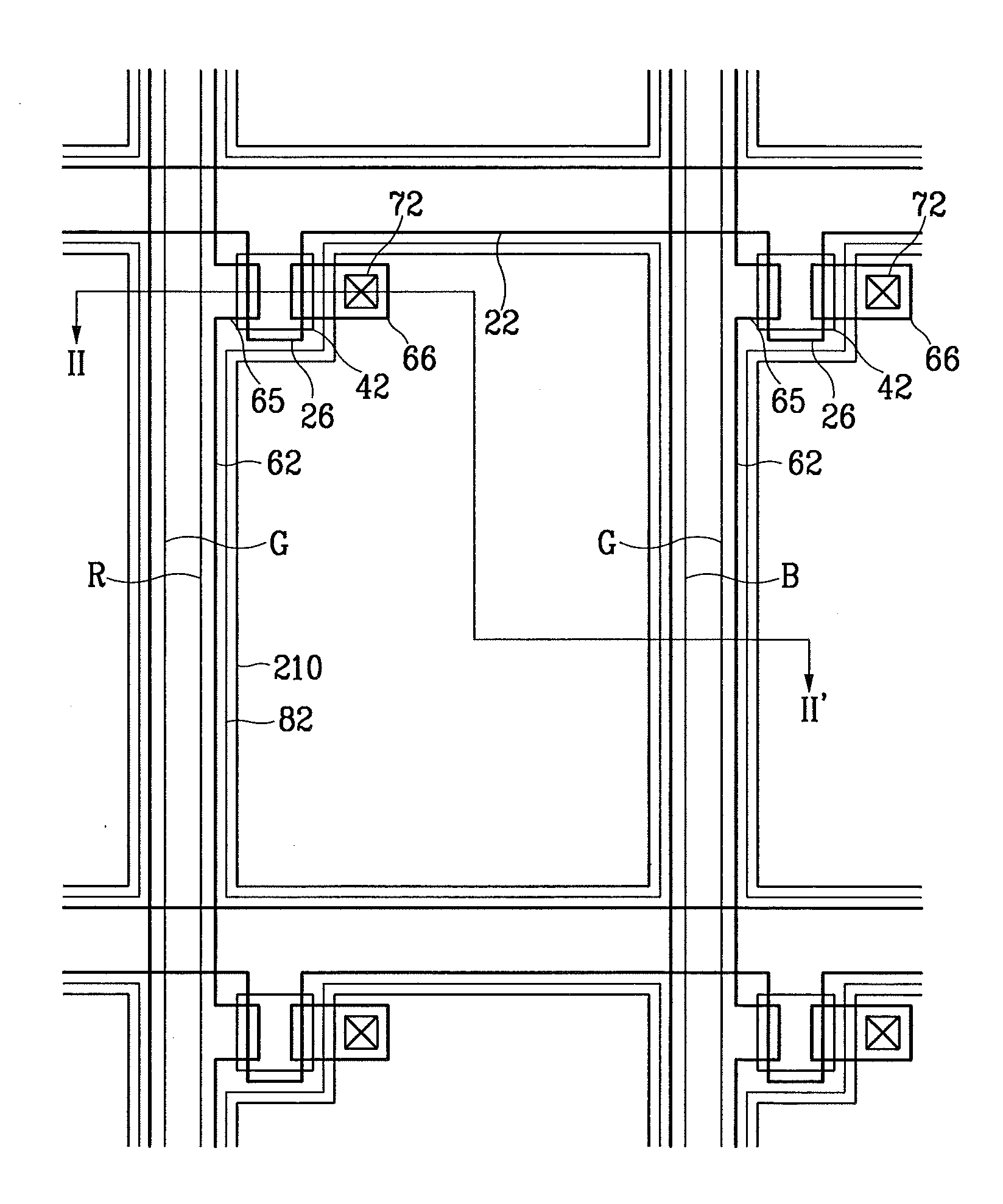
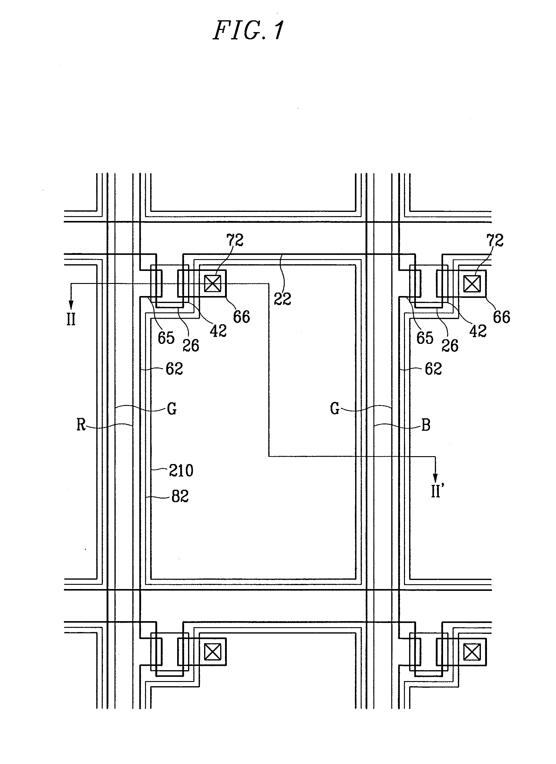
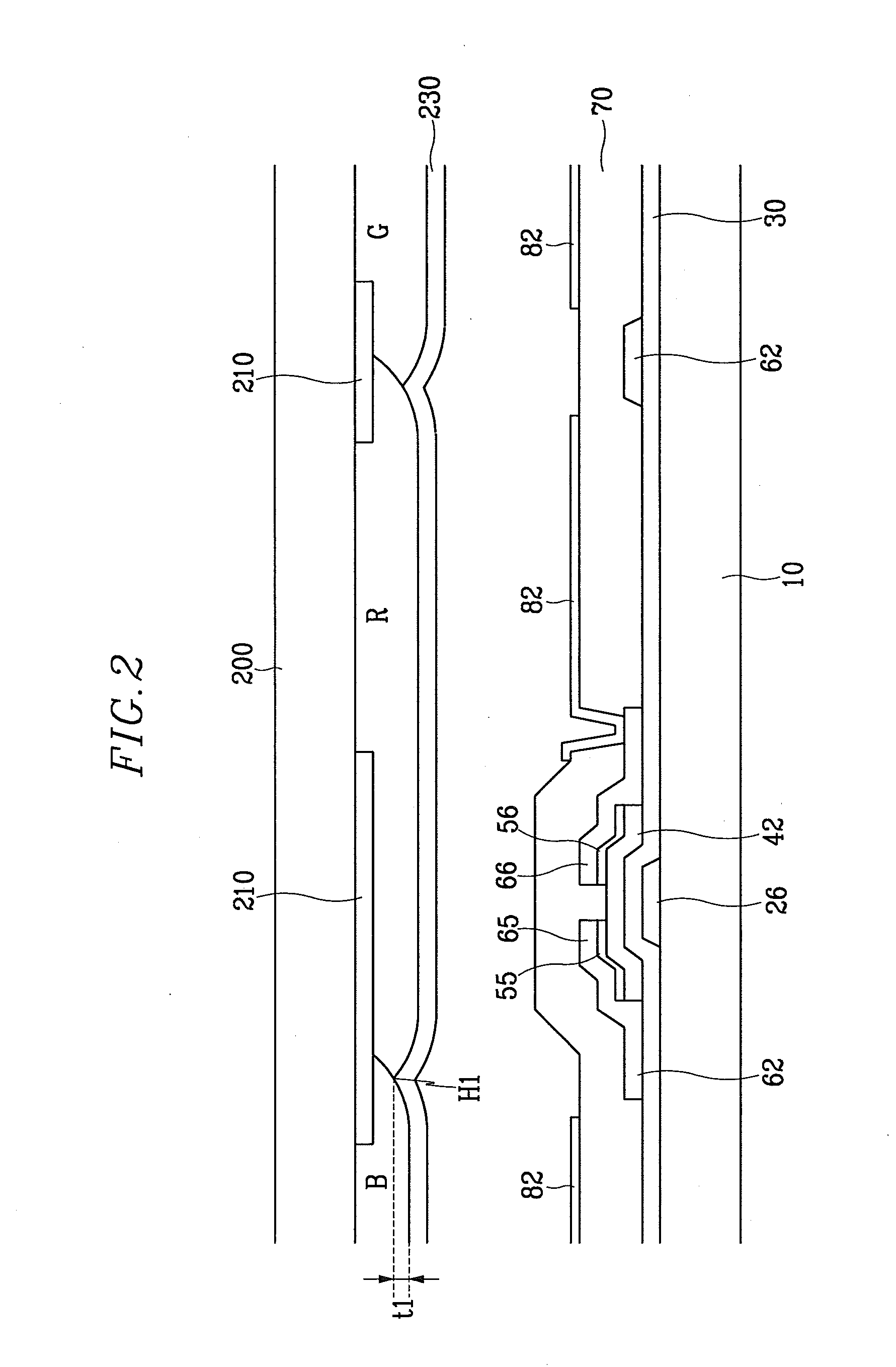
[0035]FIG. 1 is a liquid crystal display with a color filter substrate according to a preferred embodiment of the present invention, and FIG. 2 is a cross sectional view of the liquid crystal display taken along the ll-ll′ line of FIG. 1.

[0036]In the thin film transistor array substrate, a gate line assembly is formed on a first insulating substrate 10 with a metallic material such as molybdenum (Mo), a molybdenum-tungsten (MoW) alloy, chrome (Cr), tantalum (Ta), and titanium (Ti). The gate line assembly includes gate lines 22 proceeding in the horizontal direction, and gate electrodes 26 connected to the gate lines 22 as parts of the thin film transistors. The gate line assembly may have a multiple-layered structure where one layer is formed with an aluminum-based conductive material bearing a low resistance, and the other layer with a material bearing a good contact characte...


PUM

PropertyMeasurementUnit
widthaaaaaaaaaa
widthaaaaaaaaaa
distanceaaaaaaaaaa

Abstract

A color filter substrate for a liquid crystal display includes a substrate, a black matrix formed on the substrate, and a plurality of color filters formed on the substrate with the black matrix. Each color filter has a flat central portion, and a peripheral portion placed on the black matrix with a thickness smaller than the central portion. A common electrode is formed on the plurality of color filters. A thin film transistor array substrate for the liquid crystal display includes a substrate, a plurality of gate lines formed on the substrate, a plurality of data lines crossing over the gate lines while defining pixel regions, a thin film transistor formed at each pixel region, and a plurality of color filters. Each color filter has a flat central portion, and a peripheral portion placed on the data lines with a thickness smaller than the central portion. Contact holes expose the drain electrodes, and pixel electrodes are connected to the drain electrodes through the contact holes.

Description

CROSS-REFERENCE TO RELATED APPLICATIONS[0001]This application is a divisional of U.S. patent application Ser. No. 09 / 977,684, filed Oct. 16, 2001, which claims priority to Korean Application No. 2001-52829, filed on Aug. 30, 2001, the entire contents of which are hereby incorporated by reference.BACKGROUND OF THE INVENTION[0002](a) Field of the Invention[0003]The present invention relates to a color filter substrate and a thin film transistor array substrate for a liquid crystal display.[0004](b) Description of the Related Art[0005]Generally, a liquid crystal display has two substrates with electrodes, and a liquid crystal layer sandwiched between the two substrates. Voltages are applied to the electrodes so that the liquid crystal molecules in the liquid crystal layer are re-oriented to thereby control the light transmission. The electrodes may be all formed at one of the substrates. Furthermore, in order to make color expressions on the screen, color filters of red, green and blue...

Claims


Application Information

Patent Timeline
Patent Type & Authority Applications(United States)
IPC IPC(8): G02F1/1335G02B5/20G02F1/1362G02F1/1368
CPCG02F1/133512G02F2001/136222G02F1/133514G02F1/136222G02F1/1335
Inventor KIM, DONG-GYU
Owner SAMSUNG DISPLAY CO LTD
Why Eureka
Try Eureka