

Method for manufacturing substrate, liquid crystal display apparatus and method for manufacturing the same, and electronic device
a technology of liquid crystal display and substrate, which is applied in the direction of photomechanical treatment, semiconductor devices, instruments, etc., can solve the problems of disadvantageous inability to make the electric resistance values of wiring portions sufficiently small, and large power consumption of liquid crystal display apparatus. , to achieve the effect of enhancing durability, reducing cost and reducing power consumption
- Summary
- Abstract
- Description
- Claims
- Application Information
AI Technical Summary
Benefits of technology
Problems solved by technology
Method used
Image

Examples
first embodiment
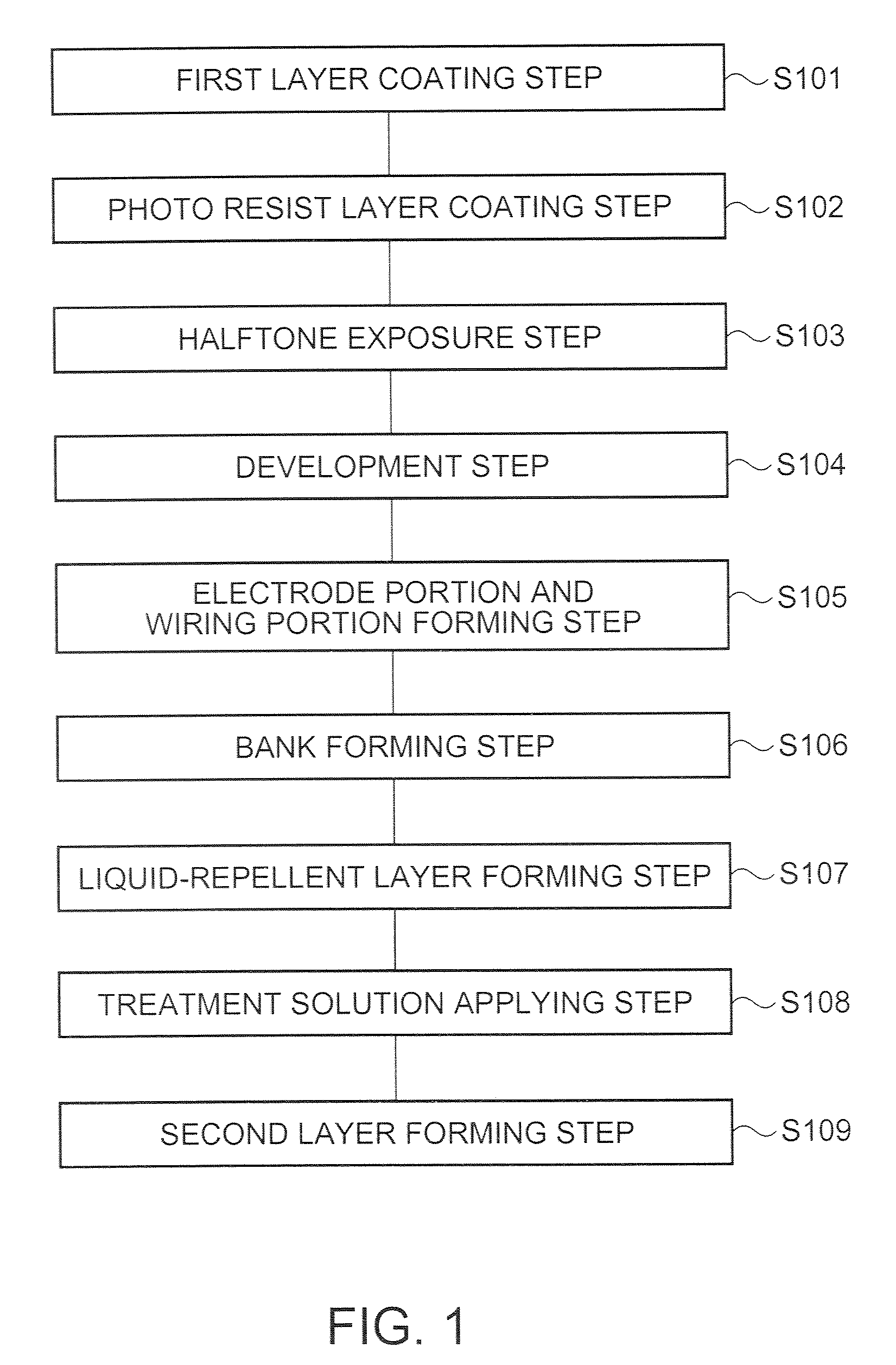
[0065]A method for manufacturing a substrate according to a first embodiment will be described below. FIG. 1 is a view showing steps of the method for manufacturing a substrate according to the first embodiment. As shown in FIG. 1, the method for manufacturing a substrate according to this embodiment of the invention includes a step S101 corresponding to a first layer coating step, a step S102 corresponding to a photo resist layer coating step, a step S103 corresponding to a halftone exposure step, a step S104 corresponding to a development step, a step S105 corresponding to an electrode and wiring portion forming step, a step S106 corresponding to a bank forming step, a step S107 corresponding to a liquid-repellent layer forming step, a step S108 corresponding to a treatment solution applying step, and a step S109 corresponding to a second layer forming step.
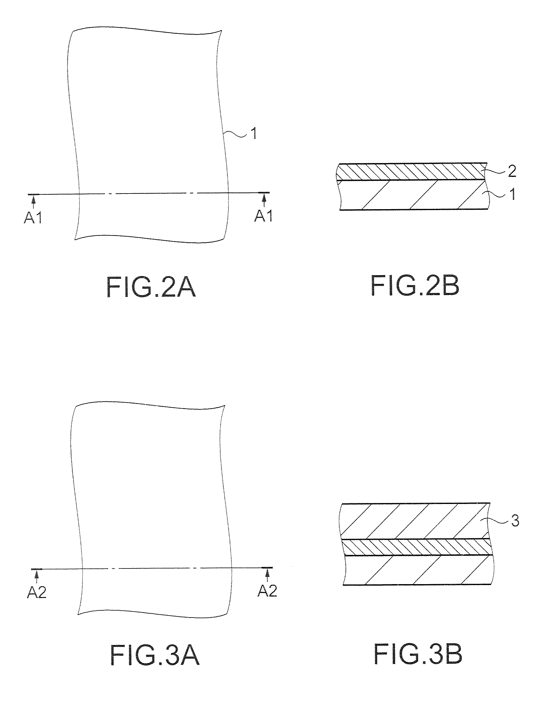
[0066]FIG. 2A through FIG. 10B are views showing respective substrates corresponding to the step S101 through S109. The expla...
second embodiment
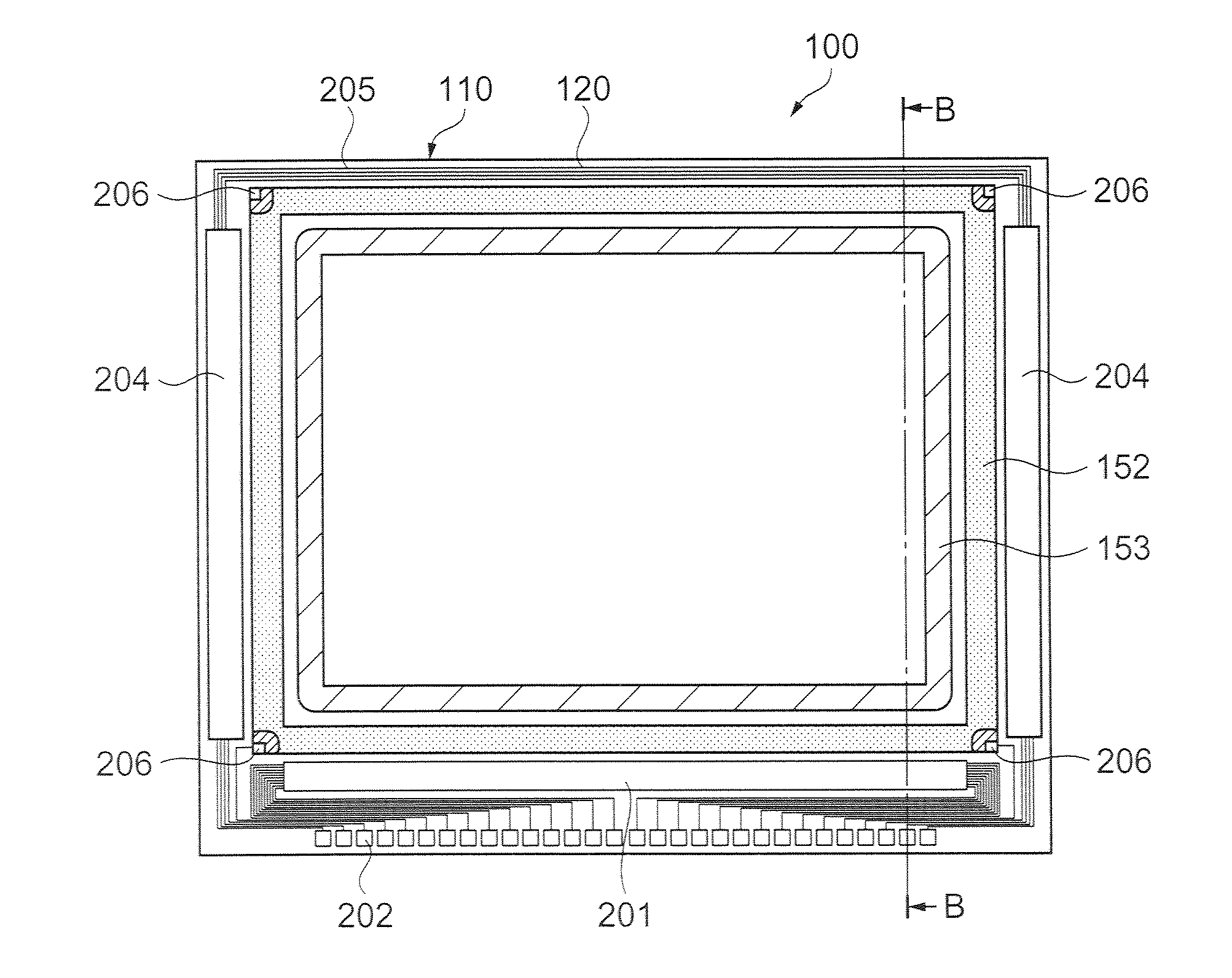
[0089]As to a second embodiment of the invention, the explanation for the same contents of the above-mentioned embodiment of the invention will be omitted and only the different contents will be described. First, a liquid crystal display apparatus according to the second embodiment will be explained. FIG. 13A is a plan view showing the liquid crystal display apparatus according to the second embodiment and FIG. 13 B is a sectional view taken along with the line B-B of FIG. 13A. As shown in FIG. 13A and FIG. 13B, in the liquid crystal display apparatus 100, a TFT array substrate 110 containing an active matrix substrate and an opposite substrate 120 are bonded with each other by a seal member 152, which is a light curing sealing agent. Liquid crystal 150 is sealed and maintained within a region defined by the seal member 152.
[0090]Formed in the region within the seal member 152 is a surrounding break line 153 made up of light shielding material. Formed in the region outside of the se...
third embodiment
[0113]As for the third embodiment of the invention, the explanation of the same contents as the above-mentioned embodiments is omitted and only the different contents will be described. FIG. 19A is a perspective view showing a cellular phone as an electronic device according to the third embodiment. FIG. 19B is a perspective view showing a portable information processing device such as a word processor or a personal computer. FIG. 19C is a perspective view showing an electronic device of wristwatch type. As shown in FIG. 19A through FIG. 19C, the cellular phone 500 includes the liquid crystal display apparatus 100 in a display portion 501. Further, the potable information processing device 600 is provided with an input portion 601 such as a key board, an information processing main body 603, and a display portion 602. This display portion 602 includes the liquid crystal display apparatus 100. Furthermore, the electronic device 700 of wristwatch type includes the liquid crystal displ...
PUM
| Property | Measurement | Unit |
|---|---|---|
| shape | aaaaa | aaaaa |
| thickness | aaaaa | aaaaa |
| metallic | aaaaa | aaaaa |
Abstract
Description
Claims
Application Information