Non-volatile memory device programming selection transistor and method of programming the same

a non-volatile memory device and programming selection technology, applied in static storage, digital storage, instruments, etc., can solve the problems of various limitations of the typical malfunction of the nand flash memory device, etc., and achieve the effect of reducing the threshold voltage distribution

Inactive Publication Date: 2009-01-29
SAMSUNG ELECTRONICS CO LTD
View PDF11 Cites 32 Cited by
  • Summary
  • Abstract
  • Description
  • Claims
  • Application Information

AI Technical Summary

Benefits of technology

[0010]The present invention provides a non-volatile memory device which reduces threshold voltage distri

Problems solved by technology

The typical NAND flash memory device therefore has various limitations due to the selection transistors

Method used


Image

  • Non-volatile memory device programming selection transistor and method of programming the same
  • Non-volatile memory device programming selection transistor and method of programming the same
  • Non-volatile memory device programming selection transistor and method of programming the same

Examples


Embodiment Construction

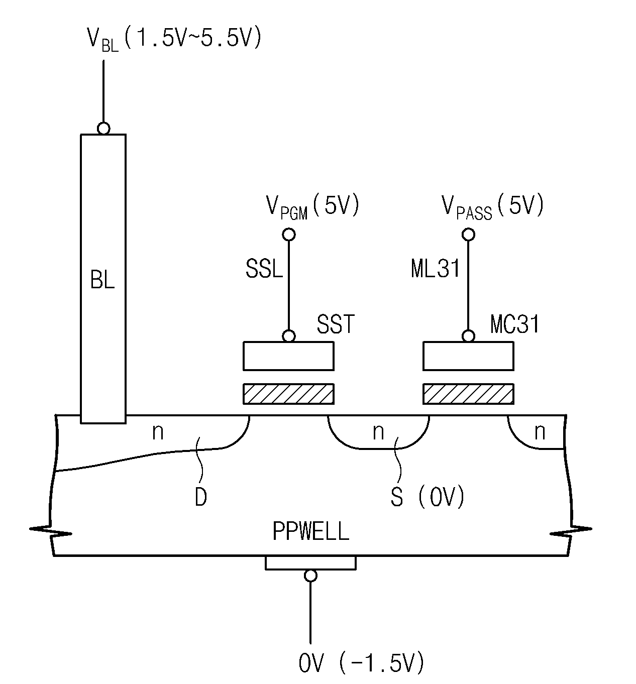
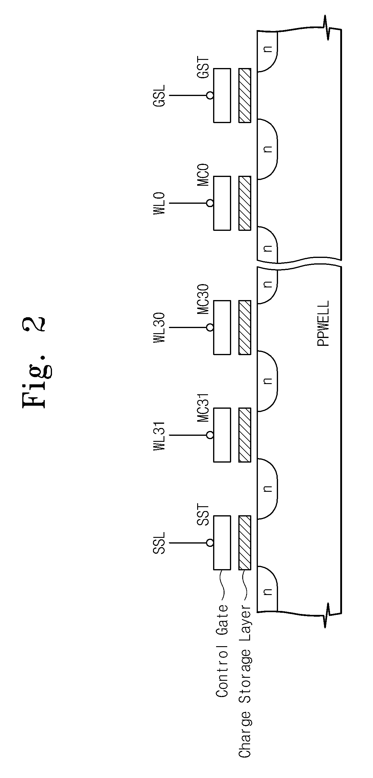
[0035]Embodiments of the present invention include methods of reducing threshold voltage distribution of a selection transistor by utilizing channel hot electron injection to program the selection transistor including a charge storage layer.

[0036]The present invention will now be described more fully with reference to the accompanying drawings, in which exemplary embodiments of the invention are shown. The invention, however, may be embodied in various different forms, and should not be construed as being limited only to the illustrated embodiments. Rather, these embodiments are provided as examples, to convey the concept of the invention to one skilled in the art. Accordingly, known processes, elements, and techniques are not described with respect to some of the embodiments of the present invention. Throughout the drawings and written description, like reference numerals will be used to refer to like or similar elements.

[0037]FIG. 2 is a sectional view illustrating a cell string s...


PUM


Abstract

A memory system includes a flash memory device and a memory controller for controlling the flash memory device. The flash memory device includes a cell string and a selection transistor connected in series to the cell string. The cell string includes multiple series-connected memory cells. The selection transistor has the same structure as a memory cell of the series-connected memory cells, and is programmed through channel hot electron injection.

Description

CROSS-REFERENCE TO RELATED APPLICATIONS[0001]A claim of priority is made to Korean Patent Application No. 10-2007-0073605, filed on Jul. 23, 2007, the subject matter of which is hereby incorporated by reference.BACKGROUND OF THE INVENTION[0002]The present invention relates to a semiconductor memory device, and more particularly, to a programming selection transistor of a non-volatile memory device, such as a flash memory device, and a method of programming the same.[0003]A semiconductor memory device is a memory device capable of storing data and reading stored data, as needed. A semiconductor memory device is typically either a random access memory (RAM) or a read only memory (ROM). The RAM is a volatile memory device which loses stored data when no power is applied. The ROM is a non-volatile memory device which retains stored data even when there is no power. Examples of RAM include dynamic RAM (DRAM) and static RAM (SRAM). Examples of ROM include programmable ROM (PROM), erasable...

Claims


Application Information

Patent Timeline
IPC IPC(8): G11C16/06
CPCG11C16/0483G11C16/3454G11C16/10G11C16/02G11C16/12
Inventor LEE, CHANG-HYUN
Owner SAMSUNG ELECTRONICS CO LTD
Why Eureka
Try Eureka