High Bandgap Arylene Polymers

a technology of arylene polymer and high bandgap, which is applied in the direction of group 3/13 element organic compounds, group 5/15 element organic compounds, and conductors, etc., can solve the problems of reducing the brightness of oleds and p-oleds as affecting the commercial application of arylene polymer, and reducing the brightness of oleds and p-oleds. a function of time, so as to

Active Publication Date: 2009-02-05
SUMITOMO CHEM CO LTD
View PDF1 Cites 4 Cited by
  • Summary
  • Abstract
  • Description
  • Claims
  • Application Information

AI Technical Summary

Benefits of technology

[0012]It is another objective of the present invention to provide OLED and p-OLED devices with improved brightness and / or lifetime.

Problems solved by technology

One cause of low efficiency is energy transfer from the excited emissive compound (whether it be fluorescent or phosphorescent, small molecule, or polymer) to a material having a lower energy excited state.
The decreasing brightness of OLEDs and p-OLEDs as a function of time is the major obstacle to commercial application.
Such chemical reactions alter the electronic properties of the emissive layer and can lead to decreases in brightness, efficiency, and (ultimately) device failure.
In fact, the lifetimes of the best polyfluorene blue phosphors are not suitable for commercial p-OLED applications.
Since excited states are more reactive than ground states the majority repeat units are prone to undergo undesired reactions.

Method used


Image

  • High Bandgap Arylene Polymers
  • High Bandgap Arylene Polymers
  • High Bandgap Arylene Polymers

Examples


Embodiment Construction

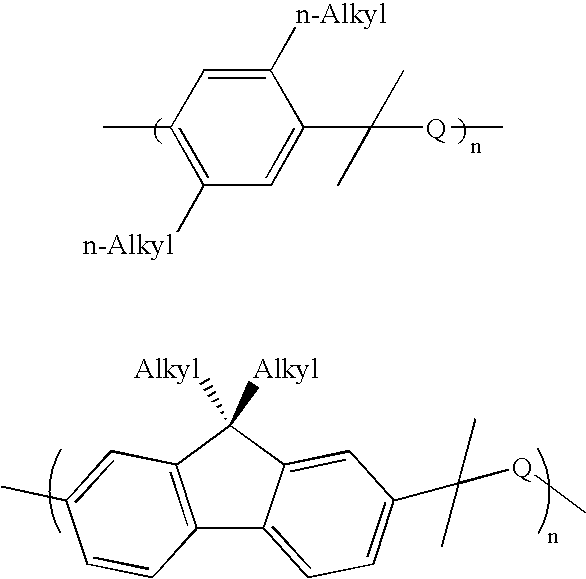
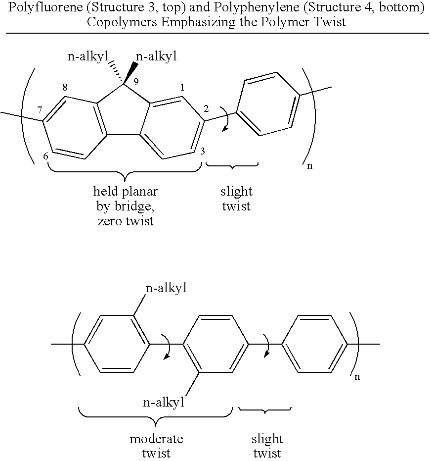
[0013]One object of the present invention is to provide a blue emissive polymer with a long lifetime. The lifetime to half brightness starting at 100 cd / m2 should be greater than 1,000 hours, preferably greater than 2,000 hours, more preferably greater than 5,000 hours, even more preferably greater than 10,000 hours, and yet more preferably greater than 20,000 hours. P-OLED devices are often tested at higher initial brightness as an accelerated ageing test. The lifetime to half brightness starting at 1,000 cd / m2 should be greater than 100 hours, preferably greater than 200 hours, more preferably greater than 500 hours, even more preferably greater than 1,000 hours, and yet more preferably greater than 2,000 hours.

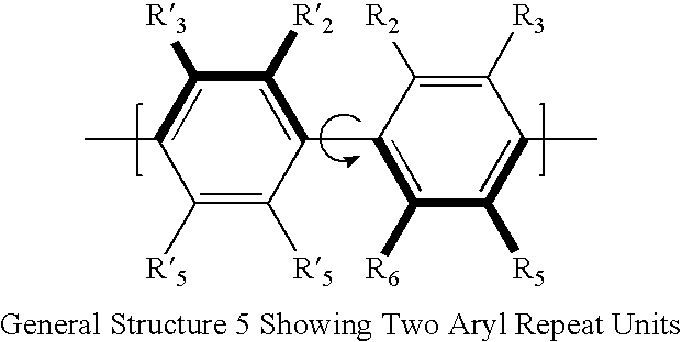
[0014]While not wishing to be bound by theory, the short lifetime of current state-of-the-art blue emissive polyphenylenes and bridged polyphenylene is likely due to the polymer serving as the emissive center. If the polymer itself has the lowest lying singlet level, then i...


PUM

PropertyMeasurementUnit
mol %aaaaaaaaaa
brightnessaaaaaaaaaa

Abstract

Luminescent polymers having sterically twisted arylene repeat units are provided, which are particularly suited as electroluminescent polymers. Monomers necessary for the synthesis of the sterically twisted polyarylene are provided, as are electroluminescent device utilizing these polymers.

Description

PRIORITY INFORMATION[0001]This application claims priority from U.S. Provisional Application Ser. No. 60 / 655,678 filed Feb. 22, 2005, which is incorporated herein by reference in its entirety.BACKGROUND OF THE INVENTION[0002]Organic Light Emitting Diodes (OLEDs) are useful in electronic displays, building lighting, signage, and other applications where efficient, lightweight, thin form-factor light sources are needed. An OLED is formed by sandwiching a fluorescent or phosphorescent organic film between two electrodes, at least one of which is transparent. Holes from the anode and electrons from the cathode recombine in the organic film and produce light. If the organic film is a polymer film the device is a polymer-OLED or p-OLED. It is known in the art how to improve efficiency of OLEDs and p-OLEDs by inclusion of various other layers in the sandwich structure, including but not limited to hole injection layers, hole transport layers, buffer layers, electron injection layers, elect...

Claims


Application Information

Patent Timeline
Patent Type & Authority Applications(United States)
IPC IPC(8): C08F230/04C08G79/08C08G73/02C07F5/02C07C211/54
CPCC08G61/02Y02E10/549C09K2211/1029C09K2211/1416C09K2211/1425C09K2211/1433C09K2211/1466C09K2211/185H01L51/0035H01L51/0039H01L51/0043H01L51/0085H01L51/5012H05B33/14C08G61/10H10K85/115H10K85/111H10K85/151H10K85/342H10K50/11C09K11/06H01B1/128H10K85/00C08G61/00H10K10/00
Inventor MARROCCO, MATTHEW L.LEE, VIRGIL J.MOTAMEDI, FARSHAD J.
Owner SUMITOMO CHEM CO LTD
Why Eureka
Try Eureka