

Vaporization of thermally sensitive materials
a thermally sensitive material and vaporization technology, applied in the field of physical vapor deposition, can solve the problems of significant degradation, changes in the structure of the molecule and associated changes in the material properties, and the degradation of organic materials used in the manufacture of oled devices, so as to reduce the probability of degradation of vaporizing materials and reduce the probability of degradation. , the effect of steady vaporization ra
- Summary
- Abstract
- Description
- Claims
- Application Information
AI Technical Summary
Benefits of technology
Problems solved by technology
Method used
Image

Examples
Embodiment Construction
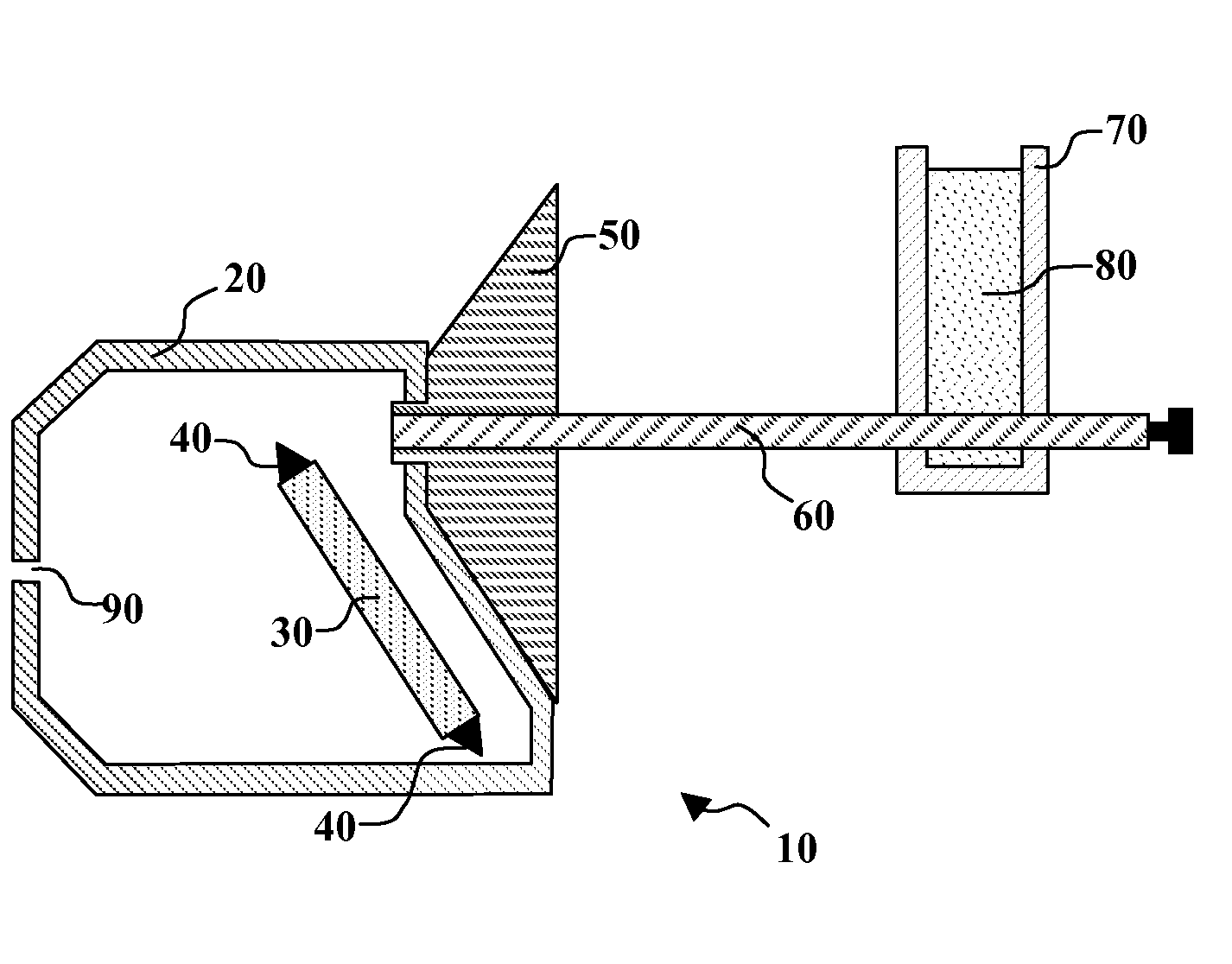
[0023]Turning now to FIG. 1, there is shown a cross-sectional view of one embodiment of a vaporizing system according to the present invention. Vaporizing system 10 includes a manifold 20 which has a heater 30, which can be held in place by supports 40. Heater 30 receives and vaporizes particulate material 80. Heater 30 has a reticulated material structure, composed of ligands that define voids in the material. The voids comprise greater than 85% of the volume of the reticulated material structure to facilitate delivery of particulate material into the voids, and conduction of vaporized material from the voids to the surrounding environment. One useful reticulated material for heater 30 is reticulated vitreous carbon. Reticulated vitreous carbon is an open-pore foam material composed of glass-like carbon ligands that define voids that can receive particulate materials. Reticulated vitreous carbon can have a void volume as great as 97%. Such material has been described, e.g. U.S. Pat...
PUM
| Property | Measurement | Unit |
|---|---|---|
| residence time | aaaaa | aaaaa |
| diameter | aaaaa | aaaaa |
| angle | aaaaa | aaaaa |
Abstract
Description
Claims
Application Information