Image sensor structure

a sensor structure and photodiode technology, applied in the direction of diodes, radiation controlled devices, semiconductor/solid-state device details, etc., can solve the problems of limiting sensitivity by quantum efficiency (qe), unable to achieve internal gains of conventional image sensors, and unable to achieve 100%

Inactive Publication Date: 2009-02-12
MICROMEDIA TECH CORP
View PDF8 Cites 40 Cited by
  • Summary
  • Abstract
  • Description
  • Claims
  • Application Information

AI Technical Summary

Benefits of technology

[0013]The invention is directed to an active pixel sensor, wherein an avalanche photodiode thin film is deposited and integrated directly on top of CMOS readout circuitry, without affecting the electrical performance of CMOS readout circuitry already made.

Problems solved by technology

For conventional image sensors, the sensitivity is limited by the quantum efficiency (QE), which is always less than 100%.
In other words, the conventional image sensors do not have internal gains.
Typically, such a reverse-bias voltage is too low to start the avalanche impact ionization.

Method used


Image

  • Image sensor structure
  • Image sensor structure
  • Image sensor structure

Examples


Embodiment Construction

[0034]Reference will now be made in detail to the present preferred embodiments of the invention, examples of which are illustrated in the accompanying drawings. Wherever possible, the same reference numbers are used in the drawings and the description to refer to the same or like parts.

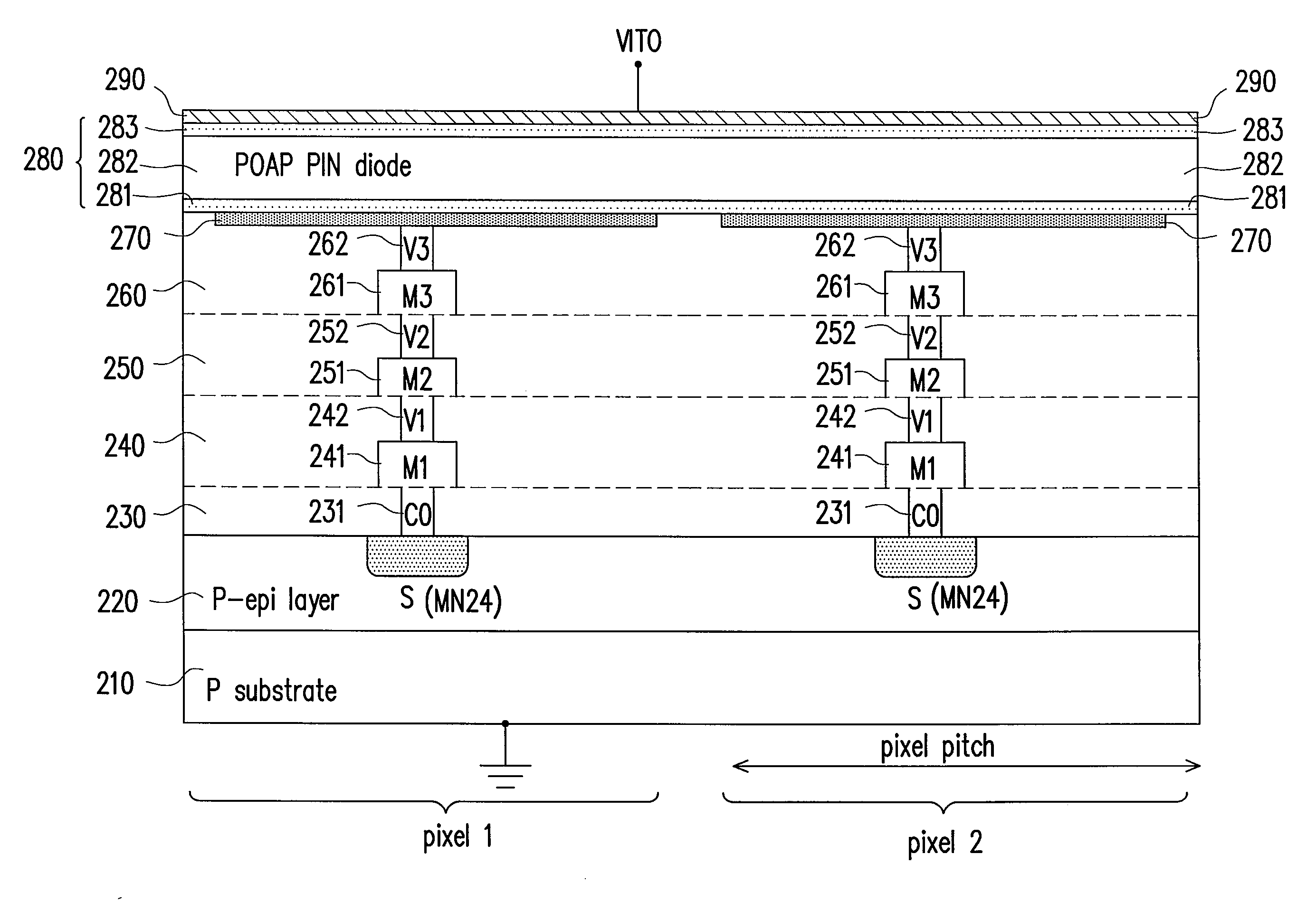
[0035]In accordance to an embodiment of the invention, an avalanche photodiode is combined with a photodiode-on-active-pixel structure to realize a new type of highly sensitive image sensor structure. The new image sensor is named as “avalanche photodiode on active pixel” sensor, or APOAP sensor.

[0036]When the photodiode is placed on top of CMOS readout circuitry (i.e., the photodiode-on-active-pixel sensor), the positive electrode of the photodiode does not need to be tied to the ground, which means the positive electrode of the photodiode may be independently biased either through an external negative voltage source, or through an internal (on-chip) negative-voltage charge pump circuit. When the re...


PUM


Abstract

An avalanche photodiode is deposited and integrated directly on top of CMOS readout circuitry. The anode of the avalanche photodiode may be independently biased at high voltage so that the avalanche photodiode may be operated in an avalanche multiplication mode. The avalanche photodiode has a multi-layered structure which is not pixilated; and photo-carrier generation and carrier multiplication may take place in the same layer or in different layers. A constant-gate-bias transistor isolates the high-voltage avalanche photodiode from the low-voltage the CMOS readout circuitry.

Description

BACKGROUND OF THE INVENTION[0001]1. Field of Invention[0002]The present invention relates to an Avalanche Photodiode On Active Pixel (APOAP) sensor structure. More particularly, the present invention relates to the integration of a thin-film avalanche photodiode structure on top of an active-pixel sensor (APS) to form a high-sensitivity APOAP image sensor.[0003]2. Description of Related Art[0004]A solid-state image sensor is a device converting light into electrical signals. Photons are first converted into electron-hole pairs, and then the photo-generated electrical charges are detected either directly as photo-currents, or indirectly as voltage changes on capacitors through the process of charge-integration over time.[0005]One of the most important features for image sensors is the light sensitivity. Sensitivity is the ratio of the voltage change to the light exposure. For conventional image sensors, the sensitivity is limited by the quantum efficiency (QE), which is always less t...

Claims


Application Information

Patent Timeline
Patent Type & Authority Applications(United States)
IPC IPC(8): H01L23/48
CPCH01L27/14643H01L27/14632
Inventor CHAO, CALVIN YI-PING
Owner MICROMEDIA TECH CORP
Why Eureka
Try Eureka