Inspection method for semiconductor wafer for reviewing defects

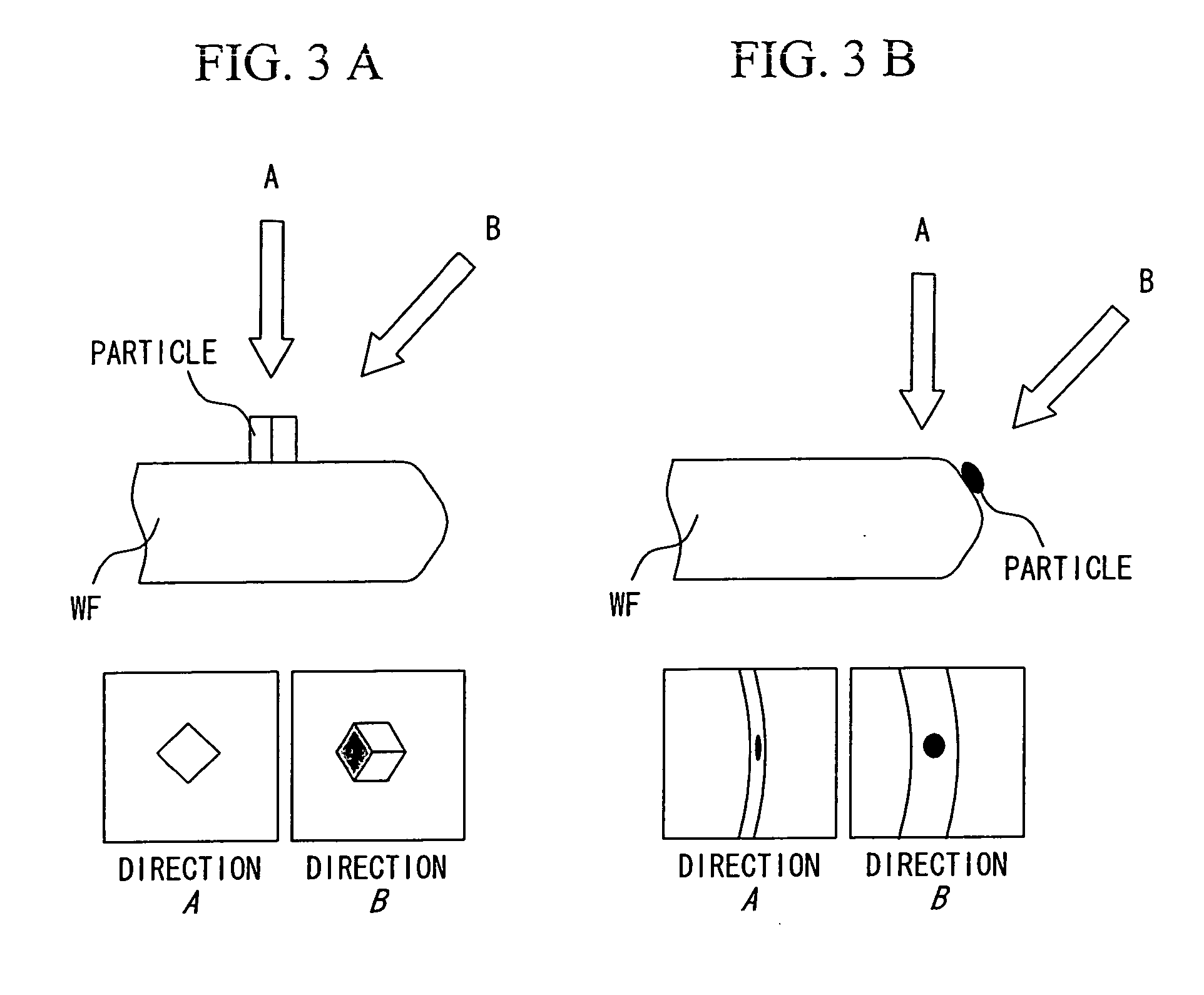
a technology of semiconductor wafers and defects, applied in the direction of material analysis, instruments, and wave/particle radiation, can solve the problems of poor adhesive electrical defects in some cases, and film easy to be easily peeled off, so as to effectively observe the edge of the wafer

Inactive Publication Date: 2009-02-19
HITACHI HIGH-TECH CORP
View PDF8 Cites 13 Cited by
  • Summary
  • Abstract
  • Description
  • Claims
  • Application Information

AI Technical Summary

Benefits of technology

[0016]According to the present invention, it is possible to effectively observe a wafer edge in a semiconductor wafer review by using an electron microscope.

Problems solved by technology

In this case, sometimes, not only the poor adhesive film tends to be easily peeled off in the process of forming the poor adhesive film, but also films tend to be easily peeled off from the outermost periphery in subsequent processes.
The films thus peeled off are adhered as particles to a processed circuit pattern, causing an electrical defect in some cases.
However, the above-describe document does not disclose a preferable technique using an electron microscope as an observation apparatus.

Method used


Image

  • Inspection method for semiconductor wafer for reviewing defects
  • Inspection method for semiconductor wafer for reviewing defects
  • Inspection method for semiconductor wafer for reviewing defects

Examples


Embodiment Construction

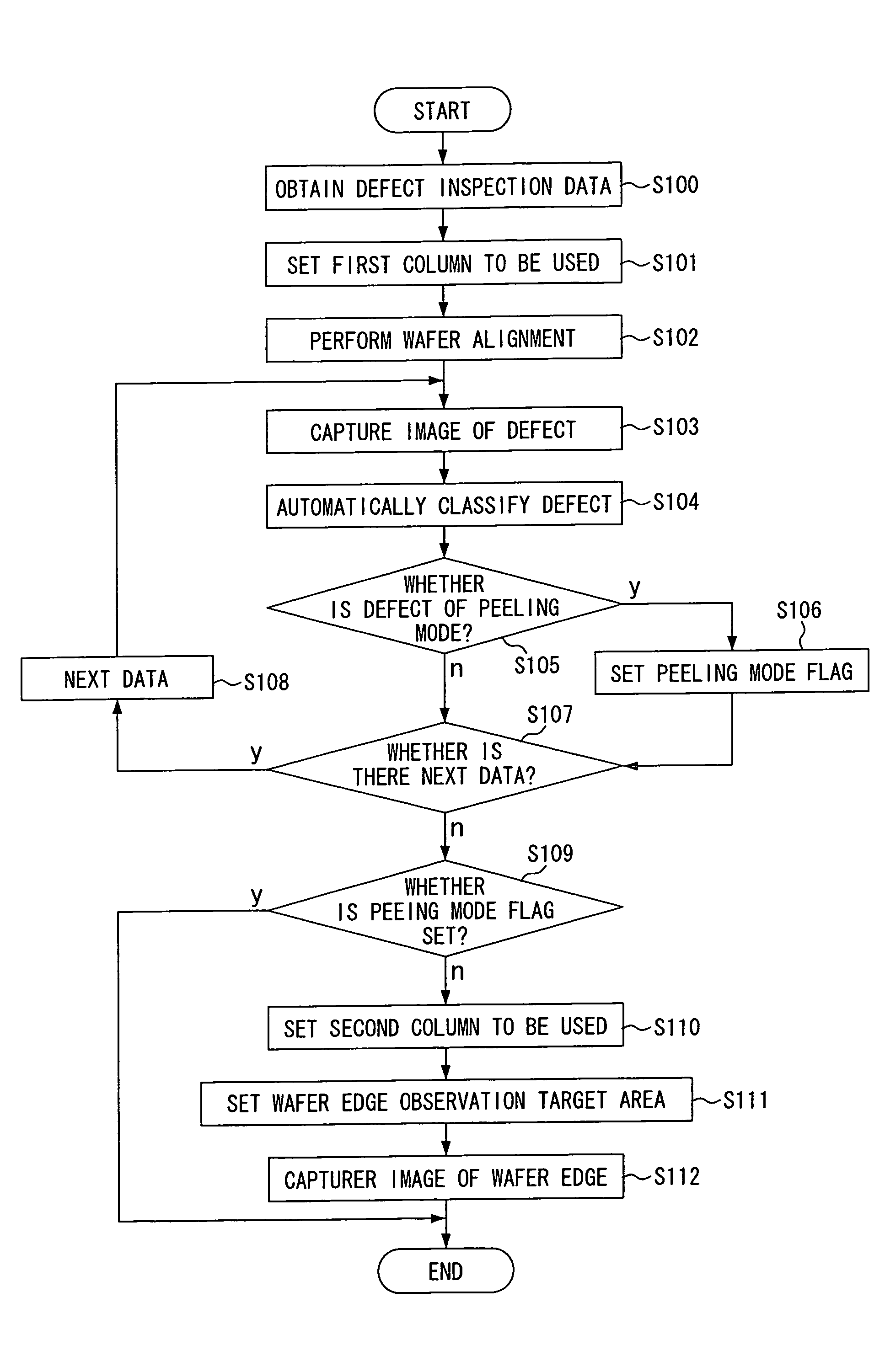
[0028]An embodiment of the present invention is described below by referring to the accompanying drawings.

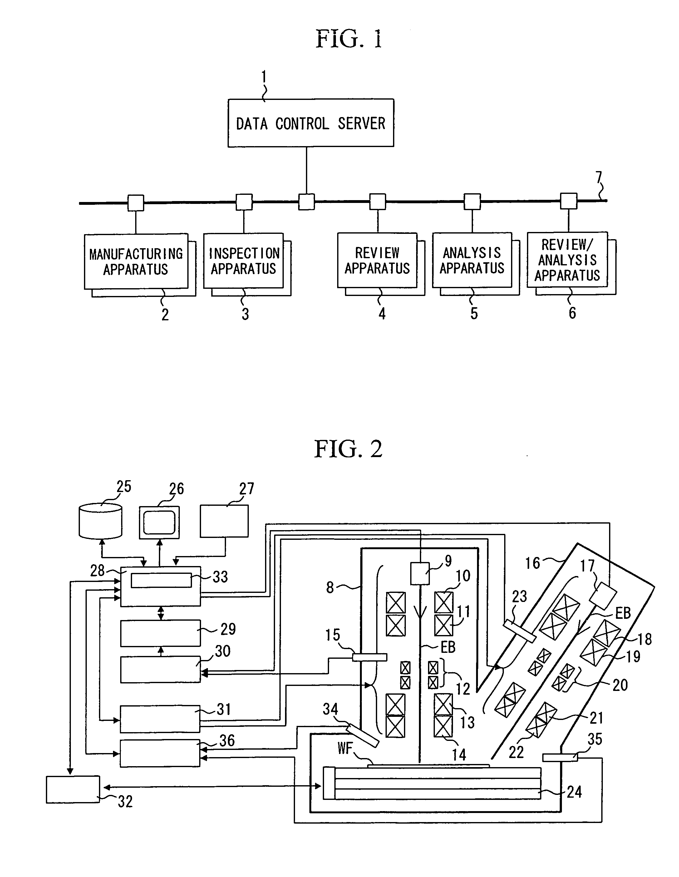
[0029]By using FIG. 1, descriptions will be given, as a specific example, of each of apparatuses on a wafer manufacturing line and a connection configuration thereof. In FIG. 1, reference numeral 1 denotes a data control server; reference numeral 2, a semiconductor manufacturing apparatus; reference numeral 3, an inspection apparatus; reference numeral 4, a review apparatus; reference numeral 5, an analysis apparatus; reference numeral 6, a review / analysis apparatus; and reference numeral 7, a network. As shown in FIG. 1, the manufacturing line has a configuration in which the semiconductor wafer manufacturing apparatus 2, the inspection apparatus 3, the review apparatus 4, the analysis apparatus 5 and the review / analysis apparatus 6 are connected to one another via the data control server 1 and the network 7.

[0030]The manufacturing apparatus 2 has a function as a lithography ma...


PUM

PropertyMeasurementUnit
semiconductor wafer inspectionaaaaaaaaaa
defect positionaaaaaaaaaa
electron beam optical systemaaaaaaaaaa

Abstract

An object of the present invention is to provide a suitable method of observing a wafer edge by using an electron microscope. The electron microscope includes a column which can take an image in being tilted, and thus allows a wafer edge to be observed from an oblique direction.

Description

CLAIM OF PRIORITY[0001]The present application claims priority from Japanese application JP 2005-352304 filed on Dec. 6, 2005, the content of which is hereby incorporated by reference into this application.BACKGROUND OF THE INVENTION[0002]1. Field of the Invention[0003]The present invention relates to a method and an apparatus for reviewing defects that have occurred in processes of manufacturing thin film devices such as semiconductor electronic circuit substrates and liquid crystal display substrates, by using a magnification image-pickup apparatus such as a scanning electron microscope.[0004]2. Description of the Related Art[0005]Manufacturing of thin film devices, such as semiconductors, liquid crystal displays, and magnetic heads for hard disks, includes a large number of processes. The number of such manufacturing processes sometimes sums to several hundreds. In a case where defects such as particles and breaks in wiring occur in thin film devices due to unsatisfactory or malf...

Claims


Application Information

Patent Timeline
Patent Type & Authority Applications(United States)
IPC IPC(8): G01N23/00
CPCH01J37/222H01J37/244H01J37/28H01J2237/24475H01J2237/2448G01N23/2251H01J2237/28H01J2237/2809H01J2237/2817H01J37/26H01J2237/24592
Inventor OBARA, KENJIHIRAI, TAKEHIRO
Owner HITACHI HIGH-TECH CORP
Why Eureka
Try Eureka