Substrate optical detection method and apparatus

An optical detection and substrate technology, applied in measuring devices, measuring electricity, measuring electrical variables, etc., can solve the problems of difficult quality control, lower process yield, high fragmentation rate, etc., and achieve the effect of avoiding fragmentation and microcracks

Inactive Publication Date: 2009-04-15
DELTA ELECTRONICS INC
View PDF0 Cites 11 Cited by
  • Summary
  • Abstract
  • Description
  • Claims
  • Application Information

AI Technical Summary

Problems solved by technology

[0004] 1. Reduced process yield: Use the current-voltage characteristic to detect microcracks. The detection of defects is after the process and before shipment, so the only treatment that can be done is scrap or downgrade, so the process yield has been reduced. For The improvement of the process does not help much, but the loss has already occurred, which directly affects the cost of materials and labor invested in production
In addition, the phenomenon of micro-cracking cannot respond to current-voltage in very slight cases, but it will make the product easy to break during handling
[0005] 2. A large number of missed inspections: With the current strong light detection technology, such as visible light as strong light irradiation, due to substrate defects may occur on the surface and inside, and most of them will not penetrate the entire cross-section of the substrate, so The strong light will not be able to penetrate the cracks that occur inside the substrate junction, that is, a large number of missed inspections will occur in the visual inspection or detection using the strong light, which will cause the problem of poor detection efficiency
[0006] 3. Difficult to control quality: the sensitivity of the current-voltage characteristic method is insufficient and it is a post-process detection, and the strong light detection is prone to a large number of missed detections, which will make it difficult to control the quality of the production line, and also form potential hazards to the process machines, such as The micro-cracks of the solar panel are broken inside the machine during the manufacturing process. In addition to affecting the production capacity, it will also cause harm to the quality of subsequent products.
[0007] 4. Unable to perform statistical process analysis: The previous technology could not effectively record the characteristics and classification of defects, and the correlation between the characteristics of defects and the manufacturing process could not be effectively collected, which was of no help to the improvement of the manufacturing process.
[0008] 5. High fragmentation rate during detection: There is no good auxiliary support or manual grasping during detection, which makes the probability of fragmentation high, resulting in waste of production

Method used


Image

  • Substrate optical detection method and apparatus
  • Substrate optical detection method and apparatus
  • Substrate optical detection method and apparatus

Examples


Embodiment Construction

[0048] The technical means of the present invention will be described in detail as follows. It is believed that the purpose, characteristics and characteristics of the present invention should be able to gain a deep and specific understanding. However, the following examples and illustrations are only provided for reference and illustration, and are not used to explain the present invention. be restricted.

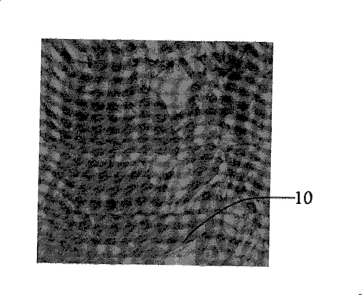
[0049] See first Figure 2A , which is a schematic diagram of the first embodiment of the optical detection device of the present invention, the optical detection device 2 includes an optical unit 21, which generates a light source 20 for irradiating a substrate 9 to detect defects of the substrate 9, wherein the light source 20 It is a light wave including any wavelength range between 700 and 1500 nanometers, and the substrate 9 is irradiated by the light source 20 to generate an image 90, which is received by an array receiving sensor unit 23 with more than one dimension...


PUM


Abstract

The invention relates to an optical detection method and a device thereof which are used for detecting the defects of a substrate. The optical detection device comprises an optical unit used for generating a light source to radiate the substrate and a plurality of groups of receiving inductor units of more than one dimension used for receiving an image generated by the radiated substrate, wherein, the light wave of the image contains a specific wavelength section as well as an image capture processing unit for capturing the image.

Description

technical field [0001] The present invention relates to an optical detection method and device, in particular to an optical detection method and device applied to substrate defect detection. Background technique [0002] The detection and analysis of substrate defects is very important in the industrial process. Taking the microcracks of solar panels as an example, there are many reasons for their occurrence, including raw material defects, handling during and between processes, etc. may cause microcracks, and Since the raw material of solar panels is mainly silicon chips, and the junction of silicon chips is easy to cause fragmentation inside or on the surface, the occurrence of fragmentation will seriously affect the process equipment, and will also affect the power generation efficiency of solar panels. [0003] At present, there are generally two ways to detect substrate defects. One is to measure the current-voltage characteristics of the substrate, and the other is to ...

Claims


Application Information

Patent Timeline
Patent Type & Authority Applications(China)
IPC IPC(8): G01R31/00G01R31/265G01R31/308
Inventor 张仁明许贸雄曾彦声何国诚杨璿俞志杰沈家麟林瑞堉
Owner DELTA ELECTRONICS INC
Why Eureka
Try Eureka