Solid state image capturing device and electronic information device

a technology of electronic information and image capturing device, which is applied in the direction of radio frequency controlled devices, television system scanning details, etc., can solve the problems of increasing parasitic capacity, affecting the output of signal lines, and the voltage subject to conversion from charge to voltage cannot be efficiently amplified to output to the signal line, so as to reduce parasitic capacity and reduce parasitic capacity , the effect of preventing shading

Inactive Publication Date: 2009-02-19
SHARP KK
View PDF2 Cites 37 Cited by
  • Summary
  • Abstract
  • Description
  • Claims
  • Application Information

AI Technical Summary

Benefits of technology

[0059]According to the present invention, the centers of respective photodiodes, which function as light receiving sections, are oriented to the centers of respective pixels, and the centers of the pixel are arranged optically at regular intervals. As a result, it is possible to prevent shading due to oblique incident light.
[0060]In the state described above, a solid-state image capturing device having a two pixel sharing structure is provided. The smaller the area for the floating diffusion FD is, the smaller the FD capacity is. Further, the shorter the FD wiring connected to the floating diffusion FD is, the smaller the parasitic capacity (wiring capacity) of the FD metal wiring is and the larger the voltage conversion gain η is. As a result, the sensitivity increases, resulting in higher resolution. More specifically, the floating diffusion FD and the reset diffusing region are positioned close to each other to be shared in a two pixel sharing structure, and further, the FD wiring, in which the floating diffusion FD and control electrodes of a signal amplifying section are connected by the first metal wiring M1 in the first layer (or the second metal wiring M2 in the second layer), is set to have a shortest layout in a substantially straight line. As a result, it is possible to significantly reduce the capacity C related to the floating diffusion FD, such as FD capacity CFD and wiring capacity Cd due to the FD wiring. Further, voltage conversion gain η is significantly improved, and it is possible to provide higher sensitivity and higher resolution for the solid-state image capturing device.
[0061]In addition, the active region area of the floating diffusion FD can be reduced by half with the two pixel sharing structure, the first metal wiring M1 is defined as the FD wiring from the floating diffusion FD to the control electrode of the signal amplifying section so as to reduce the wiring capacity, and the centers of the photodiodes are oriented to the centers of the pixels to arrange the centers of the pixel optically at regular intervals. Although the effect of reducing the capacity C related to the floating diffusion FD is even smaller, it is possible to significantly reduce the capacity C related to the floating diffusion FD, such as FD capacity CFD in the two pixel sharing structure and wiring capacity Cd due to the FD drawn wiring, and it is possible to improve the voltage conversion gain η. As a result, it is possible to provide the solid-state image capturing device with a high sensitivity and a fine resolution. Further, the two pixel sharing structure alone has an effect to reduce the capacity C related to the floating diffusion FD.
[0062]With the structure described above, the present invention makes it possible to prevent shading due to oblique incident light by orienting the centers of the photodiodes to the centers of the pixels and arranging the centers of the pixel optically at regular intervals. In this state, the floating diffusion FD and the reset diffusing region are combined together to be shared in a two pixel sharing structure, and further, the drawn wiring between the floating diffusion FD and the gate of the amplifying transistor is connected by the first metal wiring M1 in the first layer (or the second metal wiring M2 in the second layer) to have a shortest layout. As a result, it is possible to significantly reduce the capacity C related to the floating diffusion FD, such as FD capacity CFD and wiring capacity Cd due to the FD drawn wiring. Further, voltage conversion gain η is significantly improved, and it is possible to provide higher sensitivity and higher resolution for the solid-state image capturing device. In addition, the S / N can be improved.
[0063]In addition, the active region area of the floating diffusion FD can be reduced by half with the two pixel sharing structure, the first metal wiring M1 is defined as the FD wiring from the floating diffusion FD to the control electrode of the signal amplifying section so as to reduce the wiring capacity, and the centers of the photodiodes are oriented to the centers of the pixels to arrange the centers of the pixel optically at regular intervals. Although the effect of reducing the capacity C related to the floating diffusion FD is even smaller, it is possible to significantly reduce the capacity C related to the floating diffusion FD, such as FD capacity CFD in the two pixel sharing structure and wiring capacity Cd due to the FD drawn wiring and it is possible to improve the voltage conversion gain η. As a result, it is possible to provide the solid-state image capturing device with a high sensitivity and a fine resolution. In addition, S / N can be improved.

Problems solved by technology

As a result, a parasitic capacity, which the FD metal wiring has between other wirings and layers, increases.
In short, even if a signal charge is transferred from the photodiode to the floating diffusion FD and the floating diffusion takes in the signal charge, the voltage subject to conversion from charge to voltage cannot be amplified efficiently to be output to the signal line.

Method used


Image

  • Solid state image capturing device and electronic information device
  • Solid state image capturing device and electronic information device
  • Solid state image capturing device and electronic information device

Examples


embodiment 1

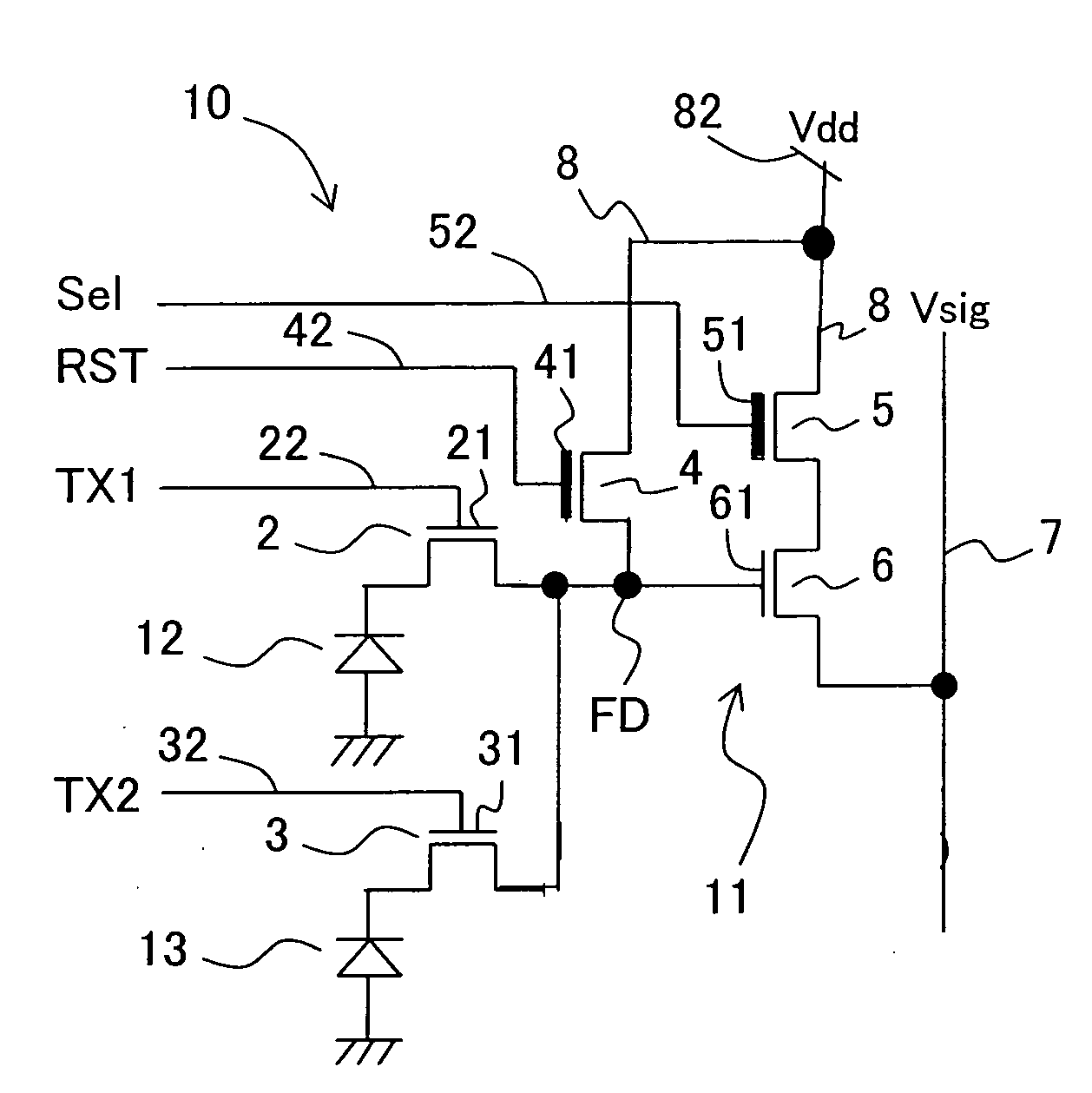
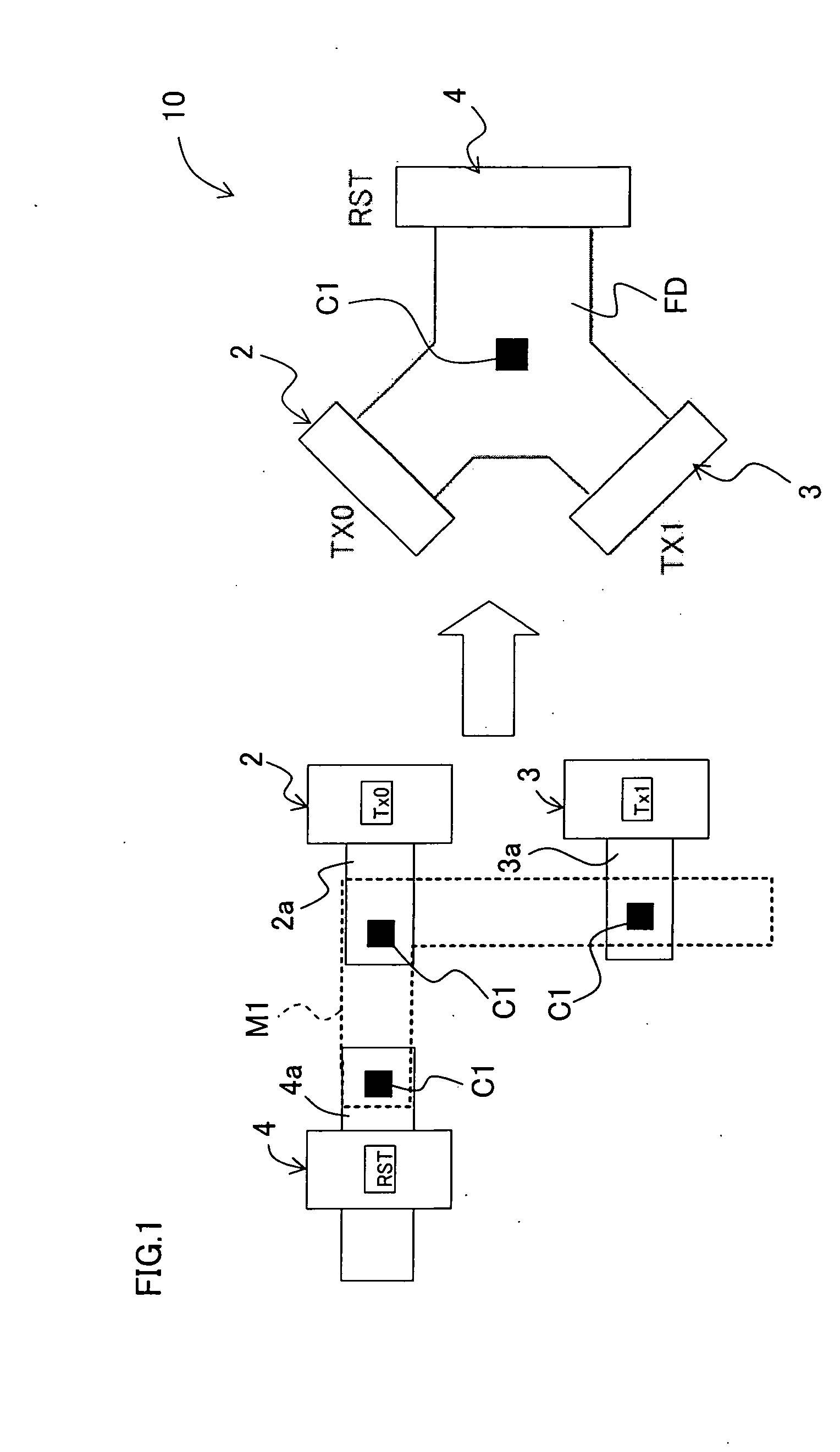
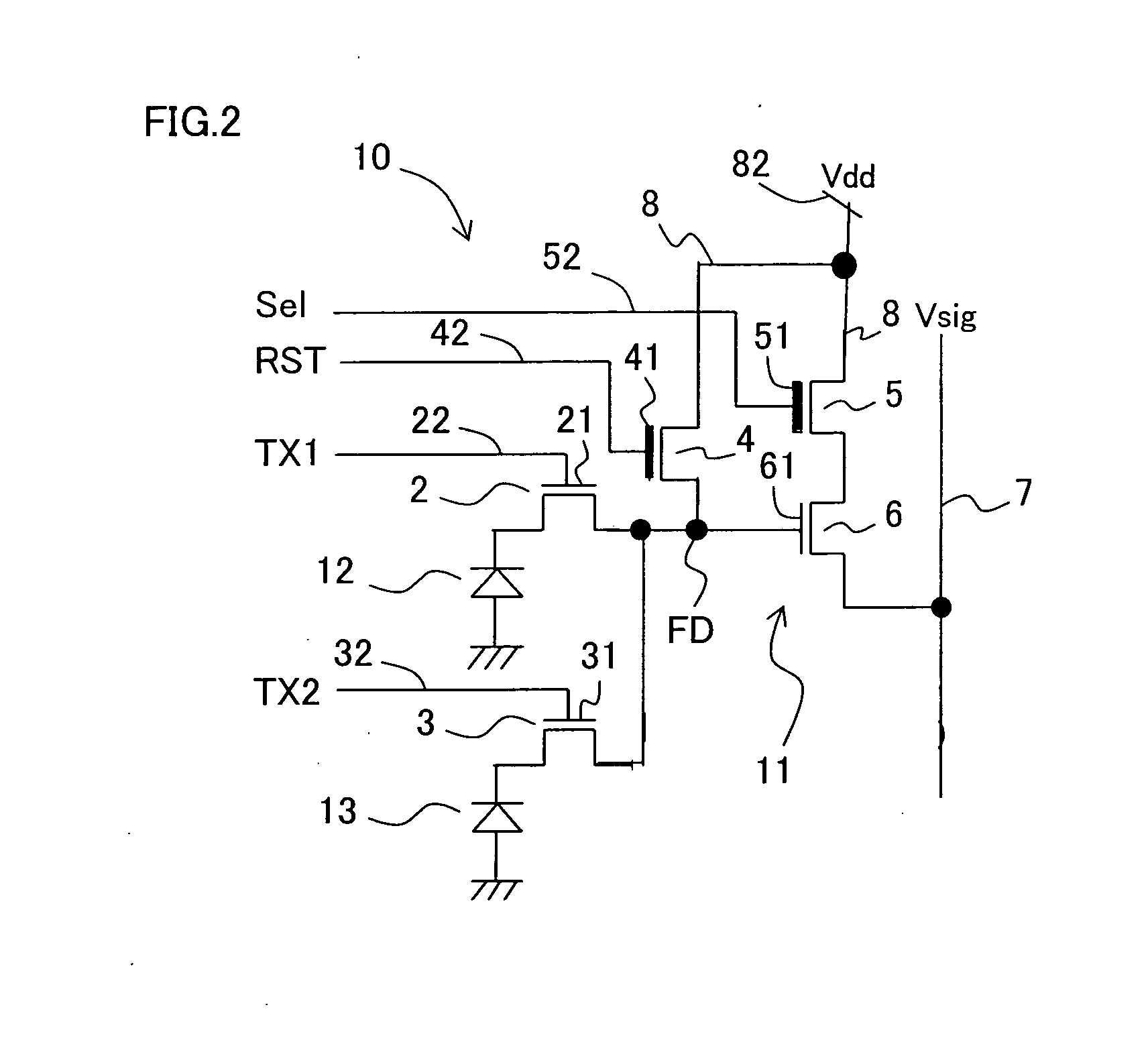
[0115]FIG. 1 is a plan view schematically showing an exemplary essential structure of a floating diffusion section in a solid-state image capturing device having a two pixel sharing structure related to Embodiment 1 of the present invention.

[0116]A conventional solid-state image capturing device having a two pixel sharing structure includes an active region 2a of a transfer transistor 2 for reading out a signal charge from a photodiode that functions as a first light receiving section, an active region 3a of a transfer transistor 3 for reading out a signal charge from a photodiode that functions as a second light receiving section, and an active region 4a of a reset transistor 4, and a floating diffusion FD is configured by connecting active region 2a to 4a with an upper layer of a first metal wiring M1 through respective contacts C1. In FIG. 1, a unit pixel section 10 in the solid-state image capturing device having a two pixel sharing structure according to Embodiment 1 does not r...

embodiment 2

[0167]According to Embodiment 1 described above, the active region area of the floating diffusion FD is reduced by half with the two pixel sharing structure, and the FD active region area is reduced by the reset transistor active region functioning as the active region of the floating diffusion FD. Further, in order to reduce the wiring capacity connected to the floating diffusion FD, the FD wiring 9, which extends from the floating diffusion FD to the gate of the amplifying transistor, is defined as the first metal wiring M1 instead of the second metal wiring M2. Further, the FD wiring has a layout in a substantially straight line with the shortest length. The centers of the photodiodes are oriented to the centers of the pixels to arrange the centers of the pixels in regular optical intervals. In Embodiment 2 of the present invention, the condition where the FD wiring 9, which extends from the floating diffusion FD to the gate of the amplifying transistor, is defined as the first m...

embodiment 3

[0170]According to Embodiment 1 described above, the active region area of the floating diffusion FD is reduced by half with the two pixel sharing structure, and the FD active region area is reduced by the reset transistor active region functioning as the active region of the floating diffusion FD. Further, in order to reduce the wiring capacity, the FD wiring 9, which extends from the floating diffusion FD to the gate of the amplifying transistor, is defined as the first metal wiring M1 instead of the second metal wiring M2. Further, the FD wiring has a layout in a substantially straight line with the shortest length. The centers of the photodiodes are oriented to the centers of the pixels to arrange the centers of the pixels in regular optical intervals. In Embodiment 3 of the present invention, the condition where the FD wiring 9, which extends from the floating diffusion FD to the gate of the amplifying transistor, is defined as the first metal wiring M1 instead of the second me...


PUM


Abstract

A solid-state image capturing device having a two pixel sharing structure is provided. A reset section for resetting electric potential of the floating diffusion to a predetermined electric potential and a signal amplifying section for amplifying a signal in accordance with voltage of the floating diffusion to read out the signal are separately arranged. An active region of the reset section is configured to function as an active region of the floating diffusion. A wiring extending from the floating diffusion to a control electrode of the signal amplifying section is formed to be a first layer of a metal wiring having a layout of a straight line with a shortest length. Centers of the light receiving sections are oriented to centers of pixels and the centers of the pixels are arranged at regular optical intervals.

Description

[0001]This Nonprovisional Application claims priority under 35 U.S.C. §119(a) on Patent Application No. 2007-202394 filed in Japan on Aug. 2, 2008, the entire contents of which are hereby incorporated by reference.BACKGROUND OF THE INVENTION[0002]1. Field of the Invention[0003]The present invention relates to a solid-state image capturing device having a multiple pixel sharing structure formed of semiconductor devices for performing photoelectric conversion on image light from a subject to capture an image of the subject; and an electronic information device, such as a digital camera (e.g., digital video camera and digital still camera), an image input camera, a scanner, a facsimile machine and a camera-equipped cell phone device, having the solid-state image capturing device having a multiple pixel sharing structure as an image input device in an image capturing section of the electronic information device.[0004]2. Description of the Related Art[0005]A MOS image sensor using a MOS ...

Claims


Application Information

Patent Timeline
Patent Type & Authority Applications(United States)
IPC IPC(8): H04N5/335H01L27/146H04N5/357H04N5/369H04N5/374
CPCH01L27/14603H01L27/14641H01L27/14643H04N25/76H04N25/75
Inventor NAGAI, KENICHI
Owner SHARP KK
Why Eureka
Try Eureka