Semiconductor device and the method of manufacturing the same

a semiconductor and semiconductor technology, applied in the direction of semiconductor devices, semiconductor/solid-state device details, electrical apparatus, etc., can solve the problems of not being able to achieve consumer application wide adoption, and achieve excellent thermal properties, high breakdown voltage, and high latch-up withstanding capability

Inactive Publication Date: 2009-02-26
FUJI ELECTRIC CO LTD
View PDF5 Cites 25 Cited by
  • Summary
  • Abstract
  • Description
  • Claims
  • Application Information

AI Technical Summary

Benefits of technology

[0069]The semiconductor device according to the invention exhibits a high breakdown voltage and a high latch-up withstanding capability. Especially, excellent thermal properties are realized in the semiconductor device according to the invention by the employment of a partial SOI structure. The manufacturing method according to the invention facilitates manufacturing a semiconductor device, having a partial SOI structure and exhibiting a high breakdown voltage, a high latch-up withstanding capability and excellent thermal properties, with low manufacturing costs.

Problems solved by technology

Moreover, since the ESD protection devices manufactured on the SOI is weaker than the protection device manufactured on the bulk wafer, it is not preferable to use the intelligent IGBT manufactured on the SOI wafer for automobiles application.
Since the SOI wafer is from 5 to 6 times as expensive as the usual bulk wafer, its wide adoption in consumer application has not yet been achieved.

Method used


Image

  • Semiconductor device and the method of manufacturing the same
  • Semiconductor device and the method of manufacturing the same
  • Semiconductor device and the method of manufacturing the same

Examples


first embodiment

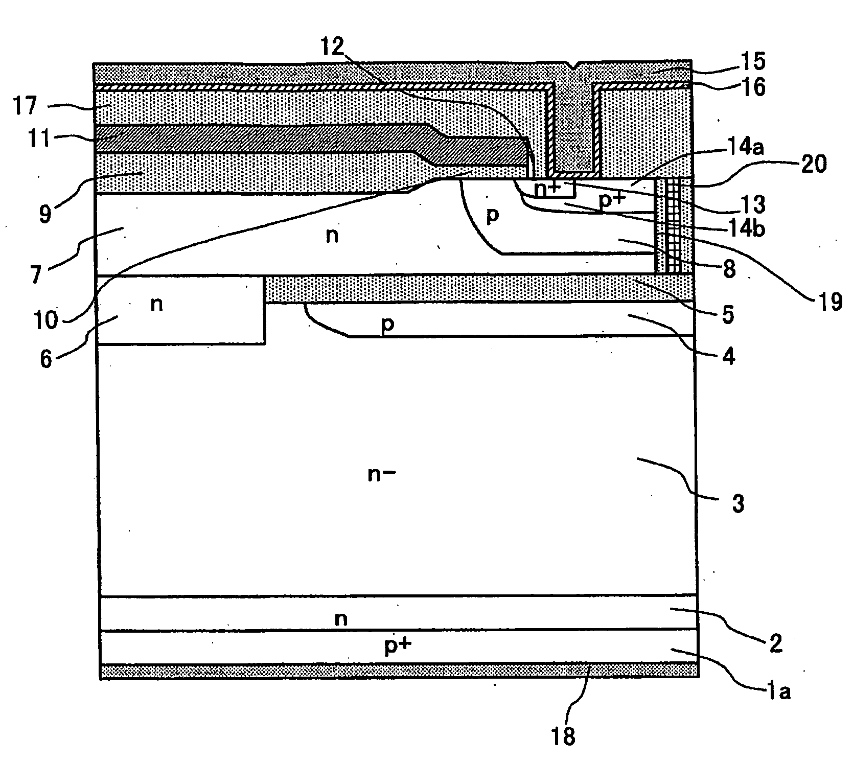
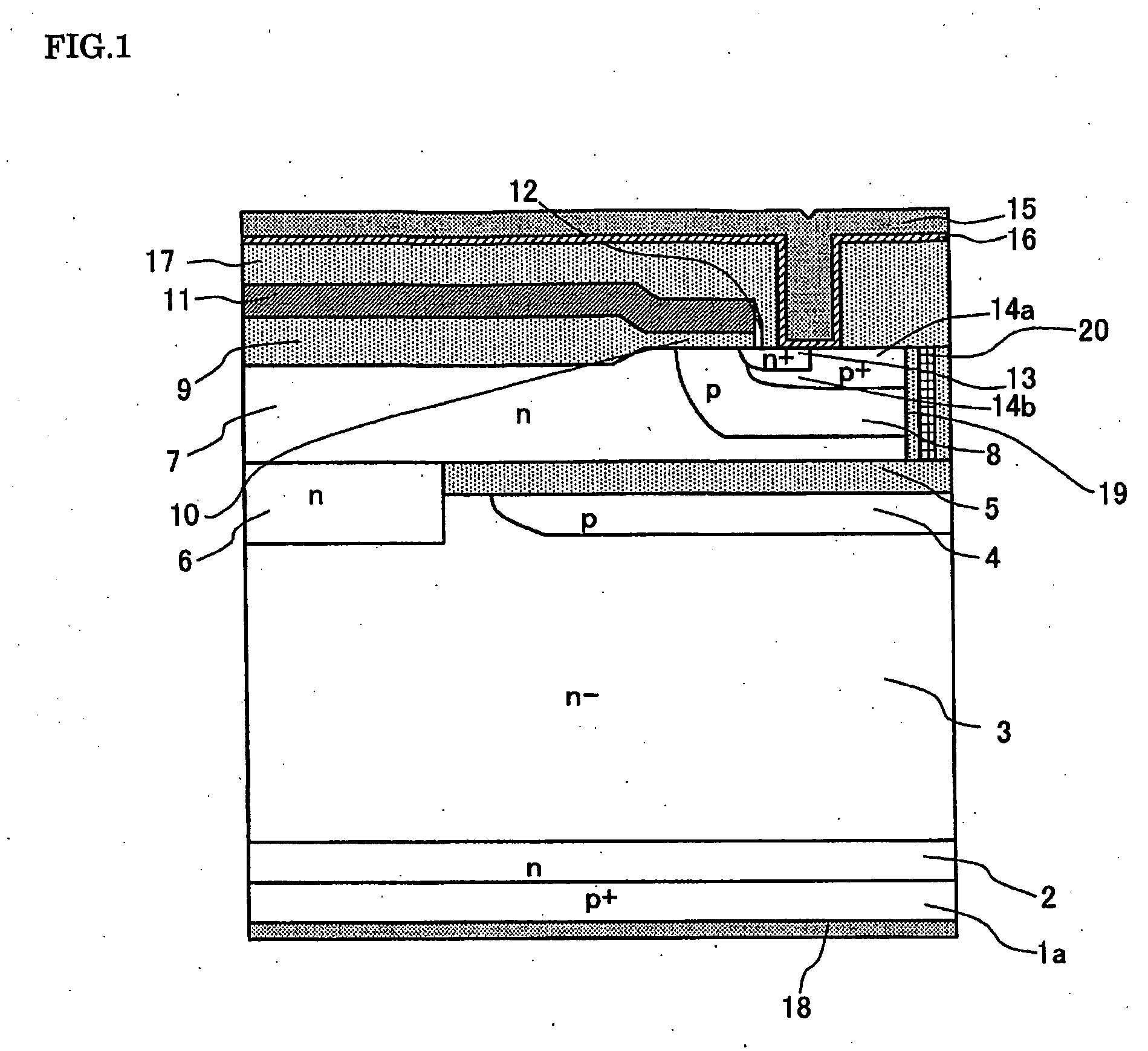
[0150]FIG. 1 is a cross sectional view of an IGBT according to the first embodiment of the invention. Referring now to FIG. 1, an n-type buffer layer 2 is disposed on a p+-type collector layer (low-resistance layer) 1a and an n−-type drift layer 3 is disposed on n-type buffer layer 2. The first n-type region 7 is above n−-type drift layer 3. A buried insulator region 5, such as an oxide film, is disposed partially between n−-type drift layer 3 and first n-type region 7, constituting a partial SOI structure.

[0151]The region between the n−-type drift layer 3 and the first n-type region7, therein any buried insulator region 5 is not present, is the second n-type region 6. The second n-type region 6 is in contact with n−-type drift layer 3 and first n-type region 7. The n−-type drift layer 3, the second n-type region 6 and the first n-type region 7 constitute the drift region (the IGBT base region) that sustains the breakdown voltage. A p-type region 4 is disposed between the buried ins...

second embodiment

[0175]FIG. 6 is a cross sectional view of an IGBT according to a second embodiment of the invention. Referring now to FIG. 6, p-type body region 8, which is spaced apart from buried insulator region 5 in the IGBT according to the first embodiment, is in contact with buried insulator region 5 in the IGBT according to the second embodiment. The other configurations in the IGBT according to the second embodiment are the same with the configurations in the IGBT according to the first embodiment. The structure according to the second embodiment is suited for the thin film devices, in which the semiconductor layer on buried insulator region 5, that is the first n-type region 7, is 1 μm or less in thickness. For applying the structure according to the second embodiment to the IGBTs, for which high-speed operations are required, it is effective to decrease the Miller capacitance and the capacitance Cgs between the gate and the source by shortening polysilicon gate electrode 11, emitter elec...

third embodiment

[0176]FIG. 8 is a cross sectional view of an IGBT according to a third embodiment of the invention. Referring now to FIG. 8, the planar gate structure in the IGBT according to the first embodiment is replaced by a trench gate structure in the IGBT according to the third embodiment. The trench gate structure is formed in the location of the IGBT, in which the trench separation structure is formed according to the first embodiment. The n+-type emitter region 13 is formed in adjacent to the trench gate structure. Since this structure makes it hard for the parasitic thyristor to work, the latch-up withstanding capability is improved. The other configurations according to the third embodiment are the same with the configurations according to the first embodiment. As illustrated in FIG. 8, p+-type buried low-resistance region 14b and gate-side-wall spacer film 12 are not disposed.


PUM


Abstract

To provide a semiconductor device that exhibits a high breakdown voltage, excellent thermal properties, a high latch-up withstanding capability and low on-resistance. The semiconductor device according to the invention, which includes a buried insulator region 5 disposed between an n-type drift layer 3 and a first n-type region 7 above n-type drift layer 3, facilitates limiting the emitter hole current, preventing latch-up from occurring, raising neither on-resistance nor on-voltage. The semiconductor device according to the invention, which includes a p-type region 4 disposed between the buried insulator region 5 and n-type drift layer 3, facilitates depleting n-type drift layer 3 in the OFF-state of the device. The semiconductor device according to the invention, which includes a second n-type region 6 disposed between the first n-type region 7 and the n-type drift layer 3, facilitates dissipating the heat caused in the channel region or in the first n-type region 7 to a p+-type collector layer 1a, which is a semiconductor substrate, via the second n-type region 6, n-type drift layer 3 and an n-type buffer layer 2.

Description

TECHNICAL FIELD[0001]The present invention relates to semiconductor devices and the method of manufacturing the semiconductor devices. Specifically, the present invention relates also to semiconductor devices having a partial SOI (silicon on insulator) structure and the method of manufacturing the semiconductor devices having a partial SOI structure.BACKGROUND ART[0002]In order to improve the performance of fuel consumption in automobiles and to purify the exhaust gas from the automobiles, engine control has been conducted electronically and the electronic engine control techniques have been advanced. An igniter is a spark plug controller that feeds electric energy to a spark plug through an ignition coil. An IGBT (insulated gate bipolar transistor) is used for the switching device of an ignition system. The IGBT is advantageous, since the driver circuit configuration for driving the IGBT is simple, the IGBT exhibits excellent protection performances against reverse battery connecti...

Claims


Application Information

Patent Timeline
Patent Type & Authority Applications(United States)
IPC IPC(8): H01L29/739H01L21/332
CPCH01L21/84H01L27/1203H01L29/0623H01L29/0653H01L29/0878H01L29/42368H01L29/7813H01L29/66333H01L29/66348H01L29/7395H01L29/7397H01L29/7802H01L29/456
Inventor LU, HONG-FEIJIMBO, SHINICHI
Owner FUJI ELECTRIC CO LTD
Why Eureka
Try Eureka