Organic electroluminescent device, method for manufacturing the same, and electronic apparatus including the same

a technology of electroluminescent devices and electronic devices, which is applied in the direction of discharge tubes/lamp details, luminescent screens of discharge tubes, synthetic resin layered products, etc., can solve the problems of short life light-emitting elements, air bubbles trapped in steps or uneven portions, and easy deterioration, so as to prevent deterioration and improve the effect of light-emitting elements

Active Publication Date: 2009-02-26
SEIKO EPSON CORP
View PDF9 Cites 37 Cited by
  • Summary
  • Abstract
  • Description
  • Claims
  • Application Information

AI Technical Summary

Benefits of technology

[0008]An advantage of the invention is that it provides an organic electroluminescent device including light-emitting elements prevented from deteriorating, and from which light can be efficiently extracted to ensure a fine pixel pitch and a wide viewing angle, and also provides a method for manufacturing the organic electroluminescent device and an electronic apparatus including the organic electroluminescent device.
[0009]According to an aspect of the invention, an organic electroluminescent device is provided. The organic electroluminescent device includes an element substrate including a plurality of light-emitting elements, each including a pair of electrodes with an organic luminescent layer therebetween, and a coating layer covering the light-emitting elements. A sealing substrate is opposed to the element substrate. The sealing substrate includes a plurality of color layers and a light-shielding layer separating the color layers from each other. The outer regions of the sealing substrate and the element substrate are bonded together with an outer region sealing layer therebetween. A filling layer is surrounded by the outer region sealing layer. The filling layer bonds the sealing substrate and the element substrate together in the region in which the light-emitting elements and the color layers are arranged. In this structure, the color layers and the light-shielding layer of the sealing substrate are covered with a surface-modifying layer made of a material having a higher surface energy to the material of the filling layer than the surface energy to the surfaces of the color layers and light-shielding layer.
[0010]In the organic electroluminescent device, the surfaces of the color layers and the light-shielding layer are covered with the surface-modifying layer improving the surface energy to the material of the filling layer. The surface-modifying layer acts as the contact surface with the liquid material of the filling layer to re

Problems solved by technology

Many of the materials of these layers easily react with water in the air and thus easily deteriorate.
If these layers deteriorate, a so-called “dark spot”, where light is not emitted, occurs in the organic EL device and is a cause of a short-life light-emitting element.
Unfortunately, air bubbles are trapped in a step or an uneven portion on the surfaces of the color layers or th

Method used


Image

  • Organic electroluminescent device, method for manufacturing the same, and electronic apparatus including the same
  • Organic electroluminescent device, method for manufacturing the same, and electronic apparatus including the same
  • Organic electroluminescent device, method for manufacturing the same, and electronic apparatus including the same

Examples


first embodiment

of Organic EL Device

[0041]An organic electroluminescent device (hereinafter referred to as organic EL device) will first be described according to a first embodiment of the invention.

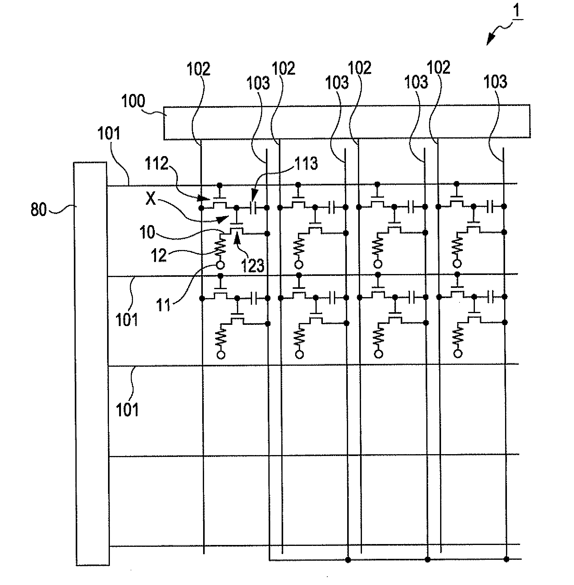
[0042]FIG. 1 is a schematic representation of the wiring structure of an organic EL device 1 according to the first embodiment.

[0043]The organic EL device 1 is of active matrix type using thin-film transistors (hereinafter referred to as TFTs) as switching elements. In the organic EL device 1, the wiring is constituted of a plurality of scanning lines 101, a plurality of signal lines 102 extending perpendicular to the scanning lines 101, and a plurality of power lines 103 extending parallel to the signal lines 102. Pixel regions X are formed in the vicinities of the respective intersections of the scanning lines 101 and the signal lines 102.

[0044]The organic EL device may not be of active matrix type using TFTs, and may be of matrix type using a simple element substrate. Such a matrix-driven organic EL ...

second embodiment

of Organic EL Device

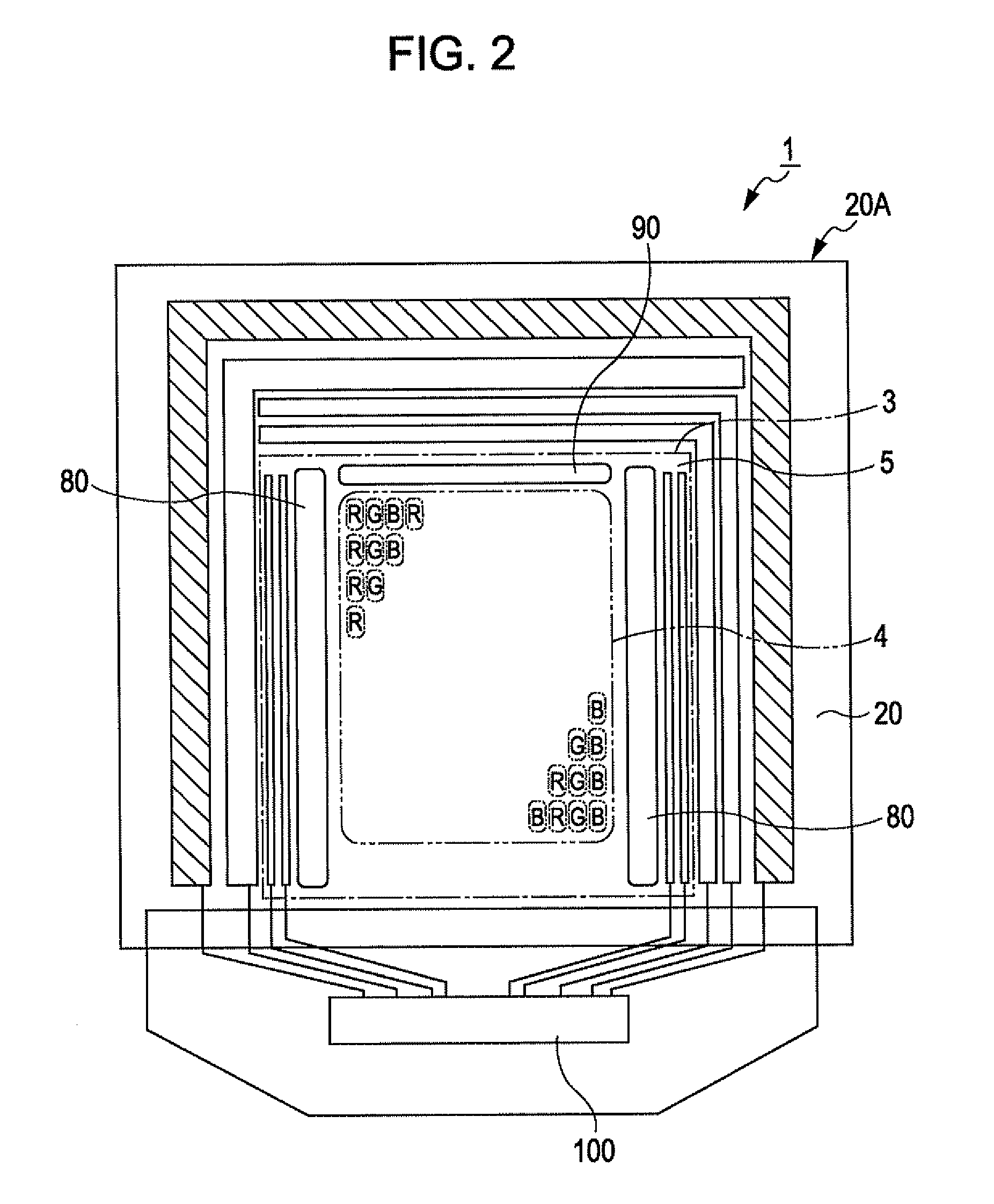
[0155]Another organic EL device 2 will now be described according to a second embodiment. The same parts in the drawings of the present embodiment are designated by the same reference numerals as in the first embodiment, and the same description is omitted. FIG. 7 is a schematic sectional view of the organic EL device 2.

[0156]The organic EL device 2 of the second embodiment is different from the organic EL device 1 of the first embodiment in that the black matrix layer 32 covers the outer region of the sealing substrate 31 corresponding to the width of the outer region sealing layer 33 in order to prevent light from leaking through the frame zone (non-light emitting region) D in the outer region of the device, and that the color layers 37 have a larger thickness than the black matrix layer 32.

[0157]By covering the outer region of the sealing substrate 31 corresponding to the width of the outer region sealing layer 33 with the black matrix layer 32 as shown in FIG...


PUM

PropertyMeasurementUnit
Thicknessaaaaaaaaaa
Pressureaaaaaaaaaa
Viscosityaaaaaaaaaa

Abstract

An organic electroluminescent device includes an element substrate including a plurality of light-emitting elements, each including a pair of electrodes with an organic luminescent layer therebetween, and a coating layer covering the light-emitting elements. A sealing substrate is opposed to the element substrate. The sealing substrate includes a plurality of color layers and a light-shielding layer separating the color layers from each other. An outer region sealing layer bonds the outer region of the sealing substrate to the outer region of the element substrate. A filling layer is surrounded by the outer region sealing layer, and bonds the sealing substrate and the element substrate together in the region in which the light-emitting elements and the color layers are arranged. The color layers and the light-shielding layer of the sealing substrate are covered with a surface-modifying layer made of a material having a higher surface energy to the material of the filling layer than the surface energy to the surfaces of the color layers and light-shielding layer.

Description

BACKGROUND[0001]1. Technical Field[0002]The present invention relates to an organic electroluminescent device, a method for manufacturing the same, and an electronic apparatus including the same.[0003]2. Related Art[0004]As information apparatuses are being diversified, lightweight, planar, power-saving display devices are increasingly desired. Among those are organic electroluminescent devices (hereinafter referred to as organic EL devices) having an organic luminescent layer.[0005]The organic EL device includes a luminescent layer, a hole injection layer, and an electron injection layer. Many of the materials of these layers easily react with water in the air and thus easily deteriorate. If these layers deteriorate, a so-called “dark spot”, where light is not emitted, occurs in the organic EL device and is a cause of a short-life light-emitting element. In order to prevent water or oxygen from permeating the light emitting elements, a structure has been proposed in which the light...

Claims


Application Information

Patent Timeline
IPC IPC(8): H01L51/52B32B37/00
CPCH01L51/5237H01L27/322H10K59/38H10K50/8426H10K50/844H01L33/52H10K50/841H10K50/84
Inventor HAYASHI, KENJI
Owner SEIKO EPSON CORP
Why Eureka
Try Eureka