Image processing device

Inactive Publication Date: 2009-02-26
MITSUBISHI ELECTRIC CORP
View PDF14 Cites 62 Cited by
  • Summary
  • Abstract
  • Description
  • Claims
  • Application Information

AI Technical Summary

Benefits of technology

[0016]Because the image processing device in accordance with the present invention includes the shader processor for carrying out the vertex shader process and the pixel shader process successively, the rasterizer unit for generating pixel data required for the pixel shader process on the basis of data on which the vertex shader process has been performed by the shader processor, and the feedback loop for feeding the pixel data outputted from the rasterizer unit back to the shader

Problems solved by technology

On the other hand, the time required for a pixel shader to perform its processing is influenced by the number of pixels included in its primitive and the degree of complexity of the pixel shader arithmetic operation.
However, when the image data to be processed is, for example, a small polygon, and the number of pixels included in this polygon is small, the processing carried out by the vertex shader causes a bottleneck to the processing carried out by the pixel shade and therefore the pixel shader enters an idle state frequently.
In contrast with this, when the image data to be processed is a large polygon, and the number of pixels included in this polygon is large, the processing carried out by the pixel shader causes a bottleneck to the processing

Method used


Image

  • Image processing device
  • Image processing device
  • Image processing device

Examples


embodiment 1

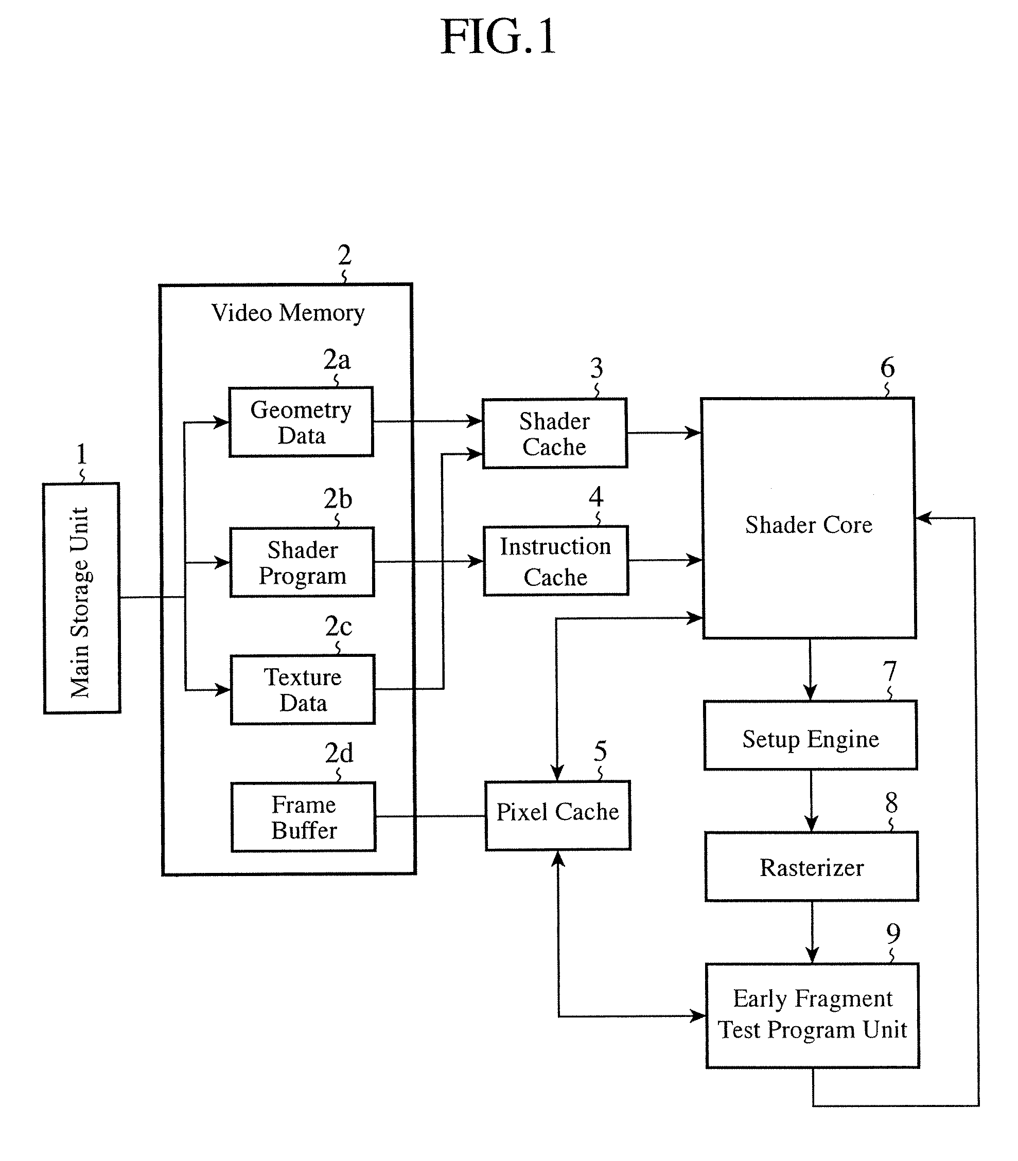
[0026]FIG. 1 is a block diagram showing the structure of an image processing device in accordance with embodiment 1 of the present invention. The image processing device in accordance with this embodiment 1 is provided with a main storage unit 1, a video memory 2, a shader cache (cache memory) 3, an instruction cache (cache memory) 4, a pixel cache (cache memory) 5, a shader core 6, a setup engine 7, a rasterizer (rasterizer unit) 8, and an early fragment test program unit (fragment test unit) 9. The main storage 1 stores geometry data 2a including vertex information which constructs an image, such as an image of an object which is a target for drawing processing, and information (data for lighting calculation) about light, including the illuminance of each light source and so on, a shader program 2b for making a processor of this image processing device operate as the shader core 6, and texture data 2c.

[0027]The video memory 2 is a storage unit intended only for the image processi...

embodiment 2

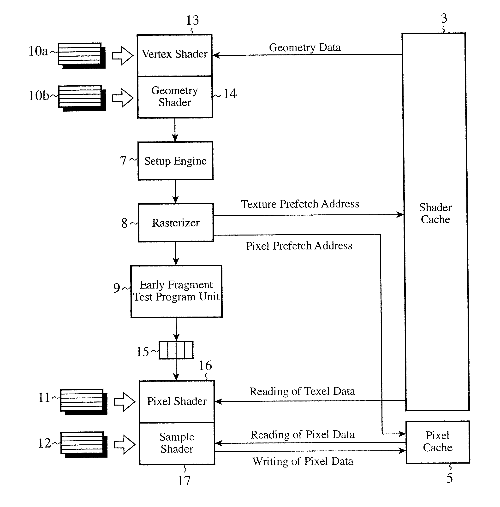
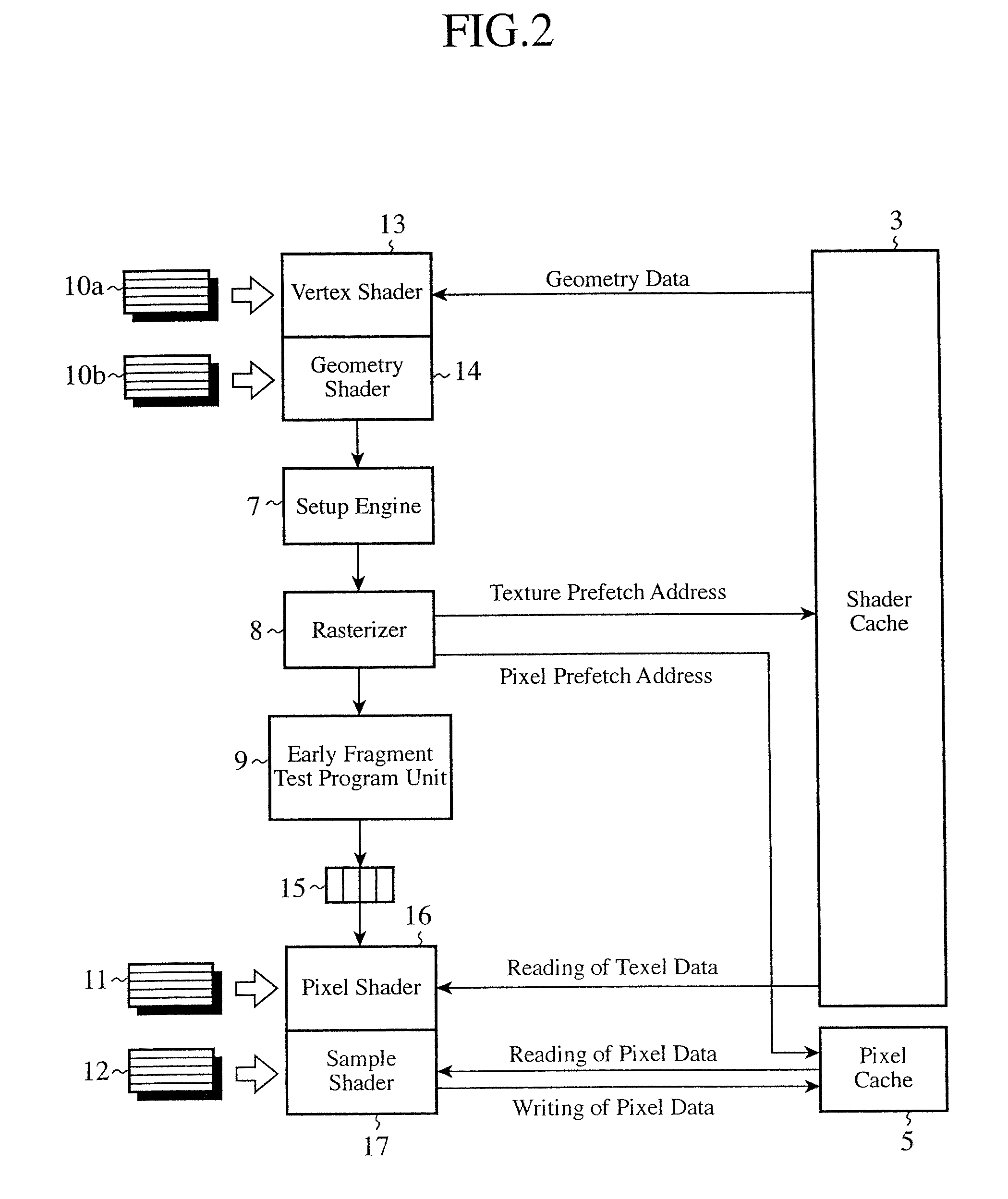
[0043]An image processing device in accordance with this embodiment 2 is so constructed as to prefetch data from the rasterizer to the shader cache and the pixel cache by using an FIFO (First In First Out) for data transfer from the rasterizer to the shader core.

[0044]FIG. 2 is a diagram for explaining the structure and the operation of a shader core of the image processing device in accordance with embodiment 2 of the present invention. In this image processing device, the FIFO 15 is disposed between the early fragment test program unit 9 which accepts the output of the rasterizer 8 and the pixel shader 16, in the structure of above-mentioned embodiment 1. In the figure, the shader core 6 is shown by a combination of a vertex shader 13, a geometry shader 14, a pixel shader 16, and a sample shader 17 in order to explain its functions, though the shader core 6 is actually constructed of a single shader processor which carries out the processes of these shaders integratedly.

[0045]The ...

embodiment 3

[0064]An image processing device in accordance with this embodiment 3 is so constructed as to carry out processes efficiently using computing units of the shader core which are configured to suit to each shader program by dynamically reconfigurating both the configuration of the computing units and the instruction set.

[0065]FIG. 5 is a diagram showing the structure of the computing units included in the shader core of the image processing device in accordance with embodiment 3 of the present invention. In the figure, the shader core 6 in accordance with embodiment 3 is provided with input registers 18a to 18d, a crossbar switch 19, register files 20 to 24, product sum operation units (computing units) 25 to 28, a scalar operation unit (computing unit) 29, output registers 30 to 34, an fp32 instruction decoder (instruction decoder) 35, an fp16 instruction decoder (instruction decoder) 36, and a sequencer 37.

[0066]For example, when the position coordinates of a pixel is processed, dat...


PUM


Abstract

An image processing device includes a shader processor for carrying out a vertex shader process and a pixel shader process successively, a rasterizer unit for generating pixel data required for the pixel shader process on the basis of data on which the vertex shader process has been performed by said shader processor, and a feedback loop for feeding the pixel data outputted from said rasterizer unit back to said shader processor as a target for the pixel shader process which follows the vertex shader process.

Description

FIELD OF THE INVENTION[0001]The present invention relates to an image processing device which displays a computer graphics image on a display screen. More particularly, it relates to an image processing device which carries out a vertex geometry process and a pixel drawing process programmably.BACKGROUND OF THE INVENTION[0002]In general, 3D graphics processing can be grouped into a geometry process of performing a coordinate transformation, a lighting calculation, etc., and a rendering process of decomposing a triangle or the like into pixels, performing texture mapping etc. on them, and drawing them into a frame buffer. In recent years, without using classic geometry processing and rendering processing which are defined beforehand by API (Application Programming Interfaces), photorealistic expression methods using a programmable graphics algorithm have been used. As one of these photorealistic expression methods, there is a vertex shader and a pixel shader (also called a fragment s...

Claims


Application Information

Patent Timeline
IPC IPC(8): G06T15/50G06T15/80
CPCG06T15/80G09G5/00G06T11/40G09G2360/18G09G2360/121
Inventor KATO, YOSHIYUKITORII, AKIRAISHIDA, RYOHEI
Owner MITSUBISHI ELECTRIC CORP
Why Eureka
Try Eureka