Semiconductor device and method of manufacture thereof

a semiconductor and semiconductor technology, applied in the direction of ion implantation coating, crystal growth process, recording by magnetic means, etc., can solve the problems of unacceptable stresses between materials affecting the device, limiting the bulk crystal material that can be grown on any given substrate, and generally not being able to provide cadmium telluride crystal material, etc., to achieve the desired crystal material more quickly, increase the consistency, and accelerate the growth rate

Inactive Publication Date: 2009-02-26
KROMEK
View PDF28 Cites 13 Cited by
  • Summary
  • Abstract
  • Description
  • Claims
  • Application Information

AI Technical Summary

Benefits of technology

[0023]Although one advantage of the present invention is the ability to produce large size crystal materials for use in large detectors or the like, it is possible to divide the substrate and crystal material grown on the substrate into smaller pieces. By producing a single, large piece of crystal and then dividing this up into smaller pieces, it is considered possible to produce the required crystal material more quickly and with greater consistency than would be the case if the smaller pieces required were formed individually.
[0024]In one embodiment, the intermediate layer can be formed using standard thin film deposition techniques. These include molecular beam epitaxy, chemical vapour deposition, sputtering, metallo organic chemical vapour deposition (MOCVD), metal organic vapour phase epitaxy and liquid phase epitaxy. Whilst all of these methods are relatively slow, since the intermediate layer is very thin, the growth rate of the layer is not of significant importance in the overall manufacturing process. In an alternative embodiment, physical vapour phase deposition techniques are used to grow the thin film intermediate layer on the substrate. When vapour phase deposition techniques are used for of growth of crystal materials, typically at a growth rate of between 100 and 500 microns / hour, it is necessary for the growth to provide an underlying layer of the same material as that to be deposited. However, when the conditions are adjusted to grow a thin film at a growth rate of between 1 and 10 microns / hour, the thin film can be grown on a foreign seed.
[0025]The transition region and bulk crystal can be deposited using the same growth technique, but with a variation in the growth parameters during the growth cycle to gradually accelerate the rate of growth. In particular, when the material is initially deposited on the substrate, the growth rate will be slow, enabling the materials to be properly nucleated and formed. After depositing this initial material, the growth parameters can be changed to increase the rate of formation of the crystal material. Where the same technique is used to form the intermediate layer, there will be an initial region where the deposition changes from the slow, thin film type, deposition to the faster, bulk crystal, deposition. This change may be a gradual change, or may be an abrupt change.
[0026]The parameters that should be changed may include at least one of the source temperature (Tsource) and the substrate temperature (Tsub). A variation in the source and / or substrate temperature will result in a change of the temperature differential (ΔT). Typically, the minimum source temperature will be around 450° C. to ensure the sublimation of the material. At temperatures lower than 450° C., no substantial sublimation will occur. The minimum substrate temperature is around 200° C. By increasing the temperature differential, for example by increasing the source temperature, the overall growth rate may be increased. It will be appreciated that the growth and sublimation temperatures are dependent on the material being deposited. For example, the growth temperature for mercury iodide is around 100 to 150° C. and the sublimation temperature is around 200 to 300° C.
[0027]It is preferred that the transition region and / or bulk crystal material is grown using a multi-tube physical vapour phase transport method, such as that disclosed in EP-B-1019568.
[0028]The seed substrate can be formed from various materials. However, preferred materials for these substrates are silicon and gallium arsenide. An advantage of forming crystals on a silicon and gallium arsenide substrate is that these substrates have good mechanical strength and commercially available at an acceptable price. This both helps ensure that the crystal material is consistently formed on the substrate, which may be more difficult with a less robust substrate, and also helps maintain the integrity of the formed material in subsequent processing, use and transportation.

Problems solved by technology

It has previously been considered that crystal mismatches between a substrate and bulk crystal material having different lattice structures prevent the formation of the bulk crystal material on such substrates, or would result in unacceptable stresses between the materials affecting the device unacceptably.
For example, it is not generally considered possible to provide a cadmium telluride crystal material, which will have a lattice parameter a=6.481 Å directly onto a silicon substrate which will have a lattice parameter a=5.4309 Å due to the lattice mismatch.
Accordingly, this limits the bulk crystal material that can be grown on any given substrate.

Method used


Image

  • Semiconductor device and method of manufacture thereof
  • Semiconductor device and method of manufacture thereof
  • Semiconductor device and method of manufacture thereof

Examples


Embodiment Construction

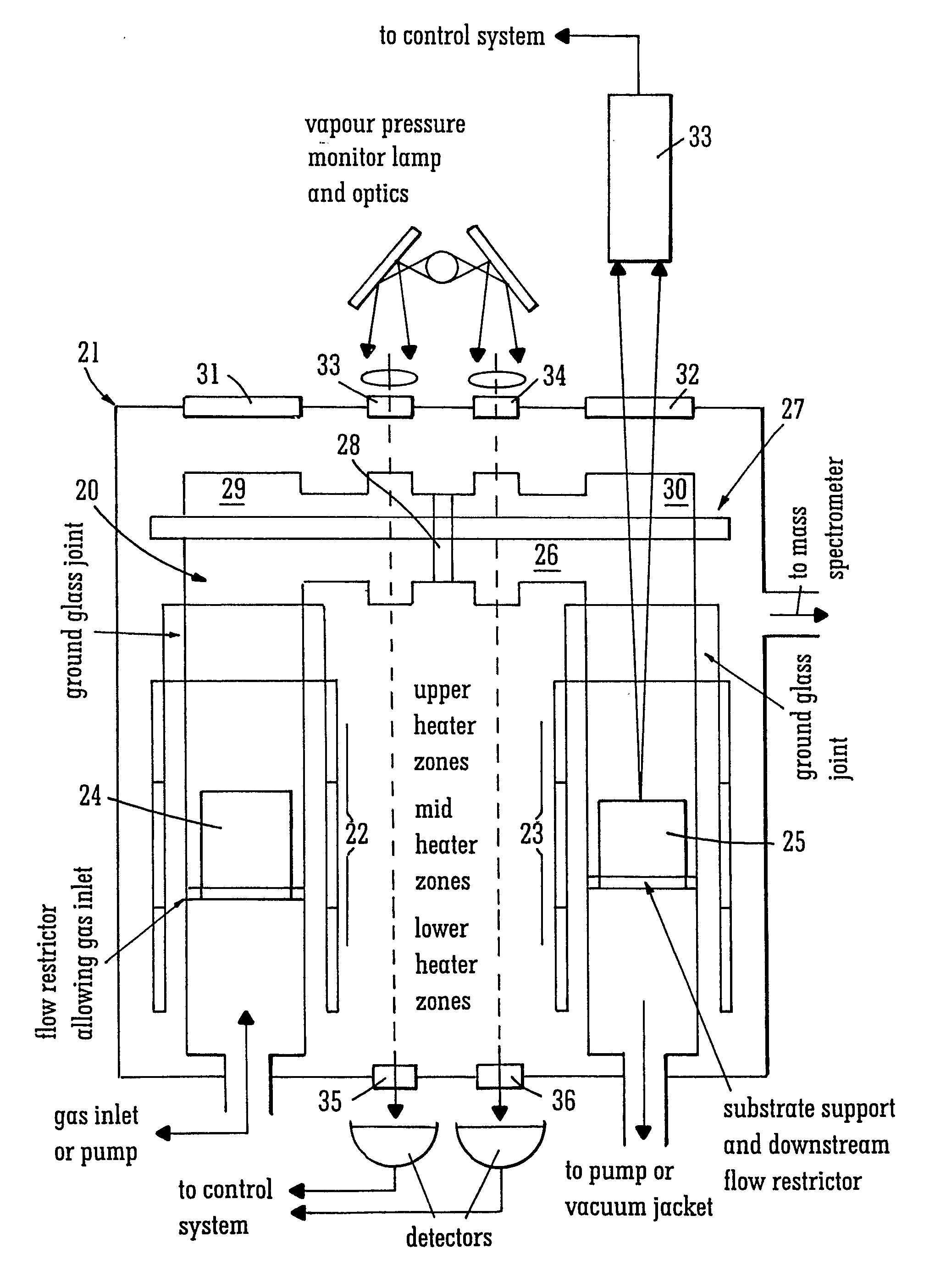
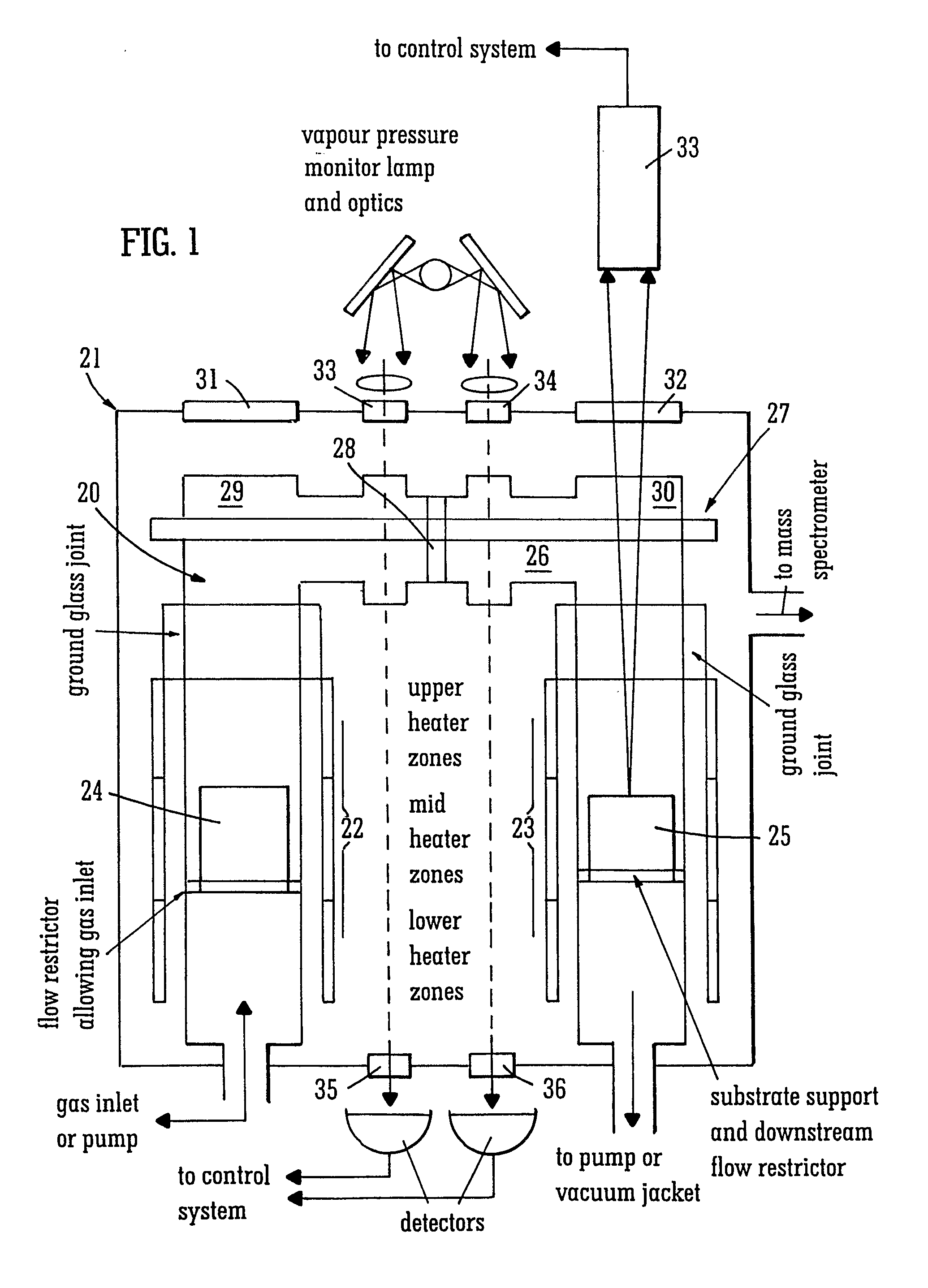
[0034]A preferred apparatus for the formation of a structure according to the present invention is shown in FIG. 1. The apparatus is suitable for forming bulk single crystal materials. Generally bulk crystal materials will have a thickness of at least 500 microns.

[0035]The apparatus comprises an evacuated U-tube in the form of a quartz envelope 20 encased in a vacuum jacket 21. Two separate three zone vertical tubular furnaces are provided 22, 23 for the source 24 and the sink zone 25 respectively. The source and sink zones are connected by an optically heated horizontal crossmember 27 forming a passage 26. A flow restrictor 28 is provided in the passage 26. The passage comprises two separate points of deviation—in each case at an angle of 90°—providing respective junctions between diverging passages for in-situ monitoring and vapour transport from the source to the sink zone. Windows allowing optical access to source and sink respectively are provided. The temperature of the surfac...


PUM

PropertyMeasurementUnit
thicknessaaaaaaaaaa
thicknessaaaaaaaaaa
diameteraaaaaaaaaa

Abstract

A structure including a substrate, an intermediate layer provided and formed directly onto the substrate, a transition region, and a group II-VI bulk crystal material provided and formed as an extension of the transition region. The transition region acts to change the structure from the underlying substrate to that of the bulk crystal. In a method of manufacture, a similar technique can be used for growing the transition region and the bulk crystal layer.

Description

FIELD OF THE INVENTION[0001]The present invention relates to a semiconductor device and a method of manufacture therefore. In particular, the present invention relates to a device comprising a group II-VI material formed on a substrate of a dissimilar material, and a method for forming such a structure.DISCUSSION OF THE PRIOR ART[0002]Single crystal materials have a number of important applications. For example, bulk cadmium telluride (CdTe) and cadmium zinc telluride (CZT) semiconductors are useful as x-ray and gamma-ray detectors which have application in security screening, medical imaging and space exploration amongst other things.[0003]For many applications, it is desired to have single crystals of large size and thickness, which can be formed rapidly with optimum uniformity and minimum impurities.[0004]Traditionally, single crystals have been formed using direct solidification techniques, such as by the Bridgman, travelling heater (THM), gradient freeze (GF) or other liquid ph...

Claims


Application Information

Patent Timeline
Patent Type & Authority Applications(United States)
IPC IPC(8): B32B9/04B32B3/02H01L21/363C23C14/34
CPCC30B11/00Y10T428/21H01L21/02378H01L21/02381H01L21/02395H01L21/02474H01L21/02477H01L21/0248H01L21/02502H01L21/02505H01L21/0251H01L21/02562H01L21/02568H01L21/02617Y10T428/266Y10T428/26C30B29/48Y10T428/31678
Inventor BASU, ARNABROBINSON, MAXCANTWELL, BENBRINKMAN, ANDY
Owner KROMEK
Why Eureka
Try Eureka