

Selective thin metal cap process
a thin metal cap and selective technology, applied in semiconductor/solid-state device manufacturing, basic electric elements, electric devices, etc., can solve the problems of difficult manufacturing of selective metal cap deposition, material of choice, aluminum, etc., and achieve the effect of improving conductivity, increasing the electrical conductivity of wiring materials, and reducing the number of wires in integrated circuits
- Summary
- Abstract
- Description
- Claims
- Application Information
AI Technical Summary
Benefits of technology
Problems solved by technology
Method used
Image

Examples
Embodiment Construction
[0012]The embodiments of the invention and the various features and advantageous details thereof are explained more fully with reference to the non-limiting embodiments that are illustrated in the accompanying drawings and detailed in the following description. It should be noted that the features illustrated in the drawings are not necessarily drawn to scale. Descriptions of well-known components and processing techniques are omitted so as to not unnecessarily obscure the embodiments of the invention. The examples used herein are intended merely to facilitate an understanding of ways in which the embodiments of the invention may be practiced and to further enable those of skill in the art to practice the embodiments of the invention. Accordingly, the examples should not be construed as limiting the scope of the embodiments of the invention.
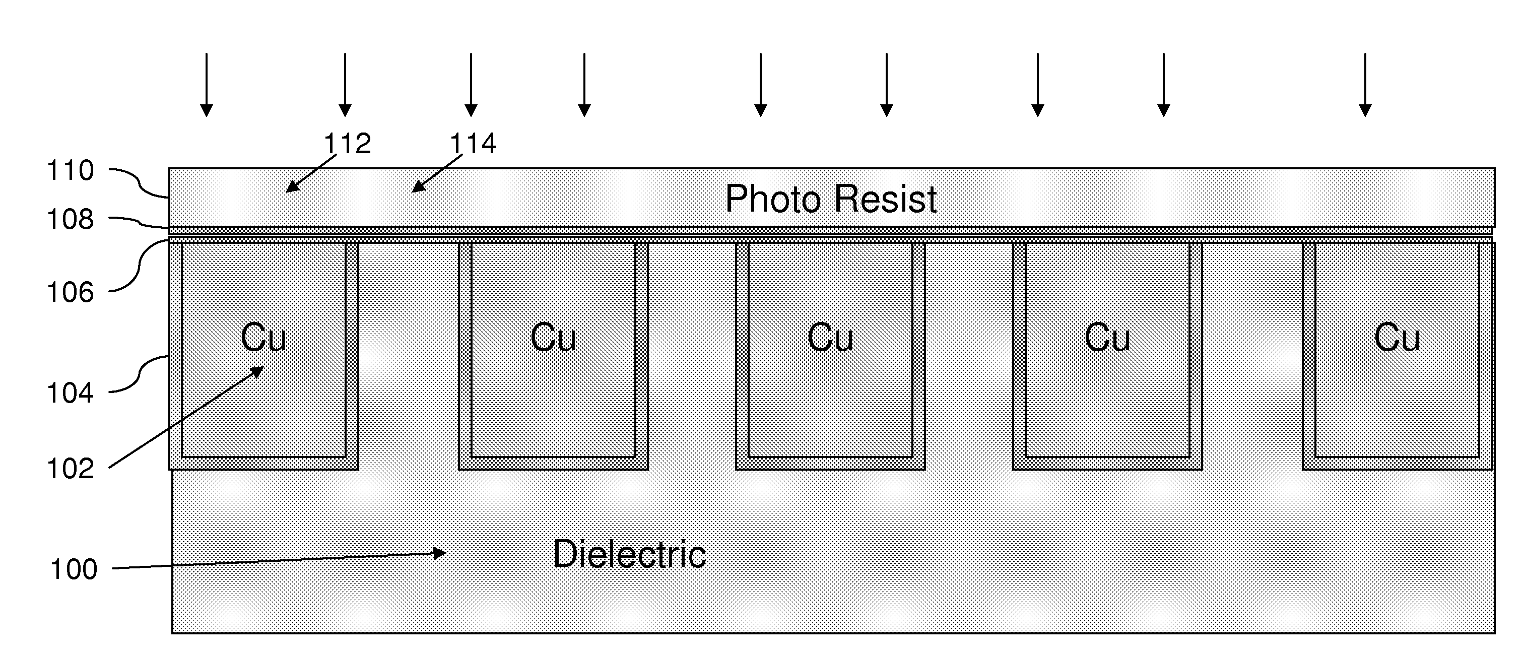
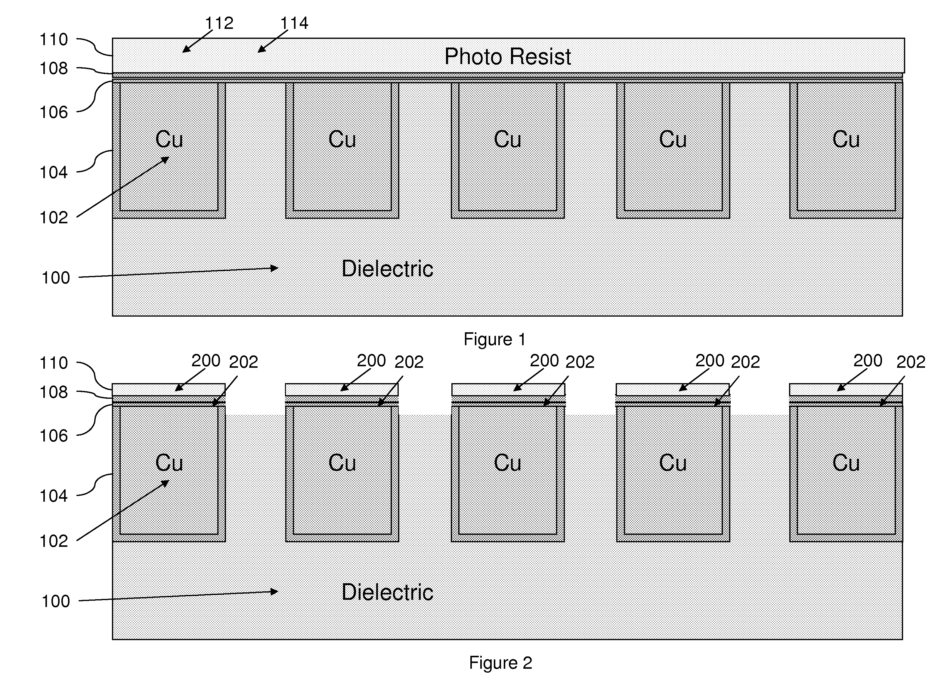
[0013]Referring now to FIGS. 1-3, a method of forming metal / dielectric hybrid caps on copper lines is illustrated. More specifically, FIG. 1 ill...
PUM
| Property | Measurement | Unit |
|---|---|---|
| thickness | aaaaa | aaaaa |
| thickness | aaaaa | aaaaa |
| electrical conductivity | aaaaa | aaaaa |
Abstract
Description
Claims
Application Information