Semiconductor Device Producing Method and Substrate Processing Apparatus

a semiconductor device and substrate technology, applied in the direction of liquid surface applicators, coatings, chemical vapor deposition coatings, etc., can solve the problems of loading effect, step coverage deterioration, and 2 /sub>film deterioration

Active Publication Date: 2009-02-26
SHIN ETSU CHEM IND CO LTD +1
View PDF5 Cites 321 Cited by
  • Summary
  • Abstract
  • Description
  • Claims
  • Application Information

AI Technical Summary

Benefits of technology

[0009]According to another aspect of the present invention, there is provided a substrate processing apparatus including: a processing chamber to process at least one substrate; a first supply system to supply the processing chamber with a metal compound or a silicon compound, each of which is a first material; a second supply system to supply the processing chamber with an oxide material which is a second material including an oxygen atom; a third supply system to supply the processing chamber with a hydride material which is a third material; an exhaust system to exhaust an atmosphere in the processing chamber; and a control section to control the first supply system, the second supply system and the third supply system so that the first material, the second material and the third material are repeatedly supplied into the processing chamber predetermined times.

Problems solved by technology

When these materials alternately flow into a reaction chamber to form the HfO2 film, there is a problem that if a pattern wafer having a trench structure is used, the step coverage is deteriorated because a film thickness is reduced at a central portion of the wafer, and coverage of the HfO2 film is deteriorated (called “loading effect”) depending upon the number of pattern wafers loaded in one batch.
However, throughput is deteriorated due to the increase in the film forming time, and COO (Cost of ownership: producing cost per one wafer) is increased due to the increase in the cost of material as a result of increased amount of the material consumed.

Method used


Image

  • Semiconductor Device Producing Method and Substrate Processing Apparatus
  • Semiconductor Device Producing Method and Substrate Processing Apparatus
  • Semiconductor Device Producing Method and Substrate Processing Apparatus

Examples


Embodiment Construction

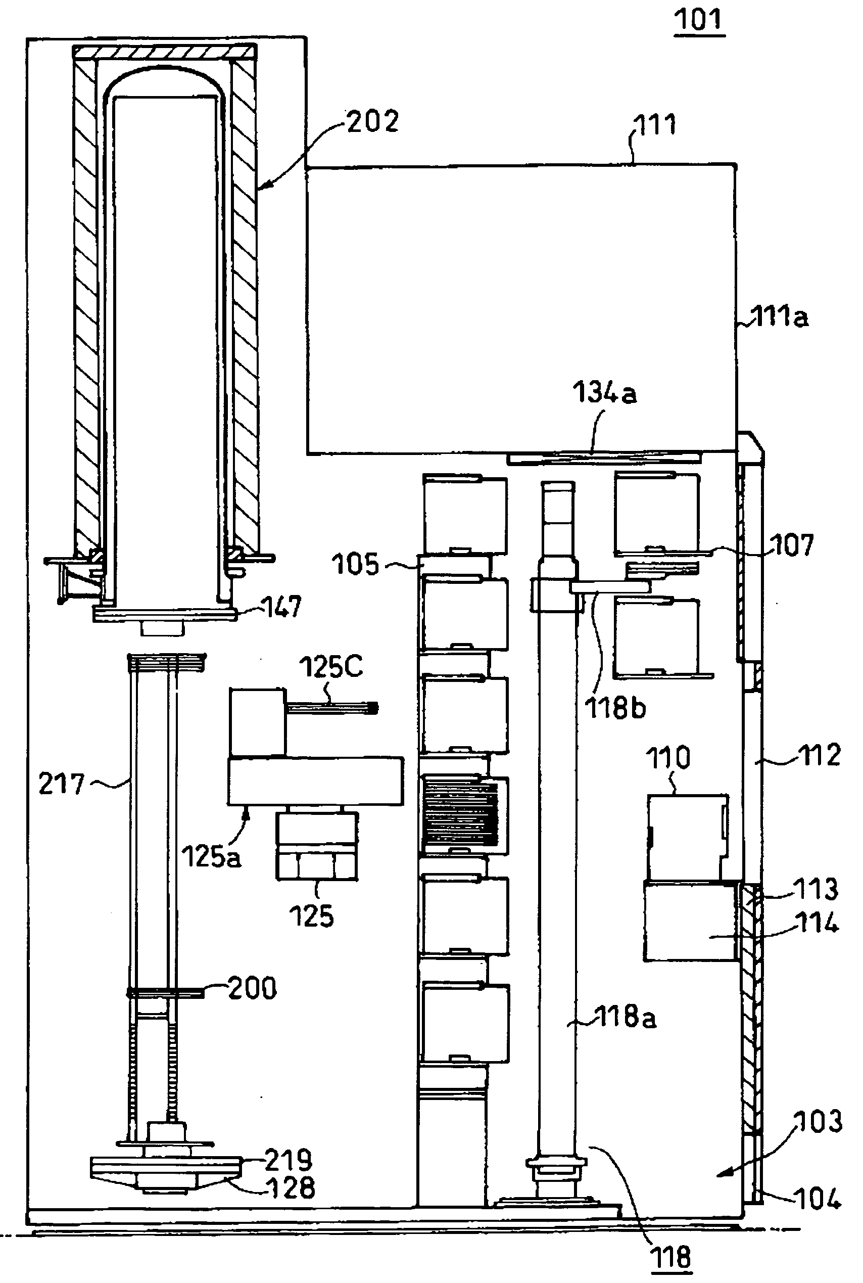
[0021]Preferred embodiments of the present invention will be explained with reference to the drawings.

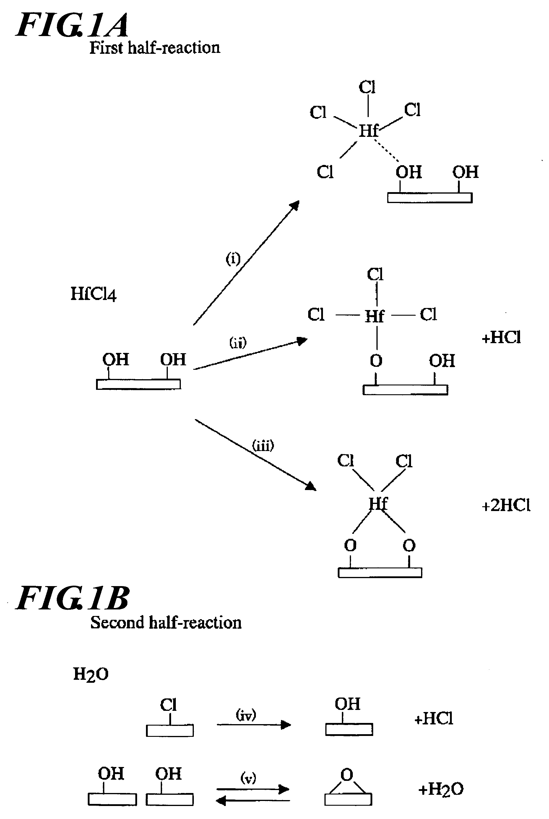
[0022]First, adsorption of a material onto a substrate when an HfO2 film is formed will be considered.

[0023]M. A. Alam and M. L. Green show that an HfO2 film forming speed in a reaction system of HfCl4 and H2O is expressed by the following equations (1) and (2) (Journal of Applied Physics, vol. 94, 2003):

dNHfO / dC=KCOVNOH  Equation (1)

dNOH / dC=K2(N0−NSiOH)+(αCOV−1)KCOVNOH  Equation (2)

[0024]Here, NHfO indicates total volume of the HfO2 film deposited per a unit area after the ALD reaction, C indicates the number of cycles of the ALD, KCOV indicates the number of hydroxyl groups (—OH) which react with HfCl4, NOH indicates a surface density of the hydroxyl group, and K2 indicates a speed constant of the hydroxyl group which is newly coupled to Si.

[0025]As shown in FIG. 1, R. L. Puurunen (Journal of Applied Physics, vol. 95, 2004) proposes a model in which Cl-groups of HfCl4 react with O...


PUM

PropertyMeasurementUnit
carbon numberaaaaaaaaaa
temperatureaaaaaaaaaa

Abstract

Disclosed is a producing method of a semiconductor device including: loading at least one substrate into a processing chamber; forming a metal oxide film or a silicon oxide film on a surface of the substrate by repeatedly supplying a metal compound or a silicon compound, each of which is a first material, an oxide material which is a second material including an oxygen atom, and a hydride material which is a third material, into the processing chamber predetermined times; and unloading the substrate from the processing chamber.

Description

TECHNICAL FIELD[0001]The present invention relates to a forming method of a thin film, a producing method of a semiconductor device and a substrate processing apparatus, and more particularly, to a technique for forming an oxide film on a semiconductor wafer (“wafer”, hereinafter) by an ALD (Atomic Layer Deposition) method in a producing method of a semiconductor integrated circuit.BACKGROUND ART[0002]In recent years, as the density of a semiconductor DRAM device is enhanced and the number of multi-layered wirings is increased, it is required to form a film at a lower temperature, and a capacitor material having excellent surface flatness, excellent recess embedding properties, excellent step coverage and a high dielectric constant (k) is required. Materials such as HfO2 (k=30) and ZrO2 (k=25) are used as a capacitor material having a higher dielectric constant than the conventional Si3N4 (k=7). There are a sputtering method, an MOCVD (Metal organic CVD) method and an ALD (Atomic la...

Claims


Application Information

Patent Timeline
Patent Type & Authority Applications(United States)
IPC IPC(8): H01L21/316B05C11/00
CPCC23C16/40C23C16/45527C23C16/45546H01L21/02164H01L21/31645H01L21/02274H01L21/0228H01L21/3141H01L21/31612H01L21/02181H01L21/20H01L21/31
Inventor MIYA, HIRONOBUHIRAHARA, KAZUHIROHAMADA, YOSHITAKASUDA, ATSUHIKO
Owner SHIN ETSU CHEM IND CO LTD
Why Eureka
Try Eureka